Genenis Gerber tools
China PCB Manufacturing, Shenzhen PCB Manufacturer, Making Circuit boards
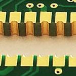
PCB Contract manufacturer, PCB Fabrication, Turnkey assembly services
Buy Print circuit board, customer: /USA/UK/Canada/South Africa...
PCB Supplier Shenzhen, China, PCB Manufacturer, Turnkey services
-
PCBSINO is the Top 5 PCB manufacturer company in China.
PCBSINO do rapid Prototype within 24 hours. we can make Flexible Print circuit boards and Rigid circuit boards, like FR4, High TG FR4, Rogers 4003, 4350,Al Aluminum metal Core MCPCB, Al2O3 Ceramic,Taconic,Halogen Free material, CEM-3, Fr2, CEM-1, CEM-2, 94VO, Rogers HF material, Polymide,Flexible PCB FPC etc.
we already made many type electronic product for our customer, Our turkey services team can source original components part for your project, senior Electronic engineer will follow each step of the production and do function test in PCB house.
Express PCB |
|
Rigid PCB Rapid Prototype,24 hours |
| Fr4 PCB |
|
prototype Lower to 15USD ! |
| Rapid Prototype |
|
Fr4 Rigid PCB Rapid Prototype China, |
Turnkey Services |
|
Turnkey PCB Assembly Services, |
| Turnkey services |
|
Print circuit board Manufacturing, Turnkey Services |
| Turnkey Assembly |
|
Through Hole PCB components wave soldering Assembly |
cadence16.5 PCB design tools
-
free download! no time limit…
TOP 9 BEST PCB DESIGN SOFTWARE OF 2017
LIYAN GONG — MARCH 13, 2017
There are many circuit design softwares available to satisfy diversified layout requirement, including free PCB design software, online free PCB design softwares, and industrial PCB softwares. This is the PCB design software list and brief introduction. You can have a comparison based on the introduction.
Contents [hide]
1 1.PROTEL( Altium Designer)
2 2. PADS (PowerPCB)
3 3. ORCAD
4 4.WG
5 5. Allegro
6 6. Eagle(Easily Applicable Graphical Layout Editor)
7 7. Kicad
8 8. EasyEda
9 9. More Free PCB Softwares
1.PROTEL( Altium Designer)
Altium Designer
5 of the best and free PCB design software platforms available
While there are a number of free programs available on the Internet, only a few are actually worth using
If you Google “design software for printed circuit boards”, you’ll get close to 2 million hits.
Google SERP
This can be a bit overwhelming for a design engineer, no matter if he / she is in the early stages of a career, or already established within a company.
PCB DESIGN - Introduction to PCB Design Library Creation
1. Introduction toIntroduction to PCB DesignPCB Design Library CreationLibrary Creation
2. Drawing the schematicDrawing the schematic • We have a new version of cadence in the lab now. You will find it listed under ALL PROGRAMS as cadence 16.1 (I am not sure if 16.1 but 16 something) • We will use design entry CIS to make the schematic • If given an option you will choose PCB design allegro in the beginning • Start a new project as we used to do in the older version
3. Drawing the schematicDrawing the schematic Click this icon to bring up the place part window Click this icon to add libraries
4. LibrariesLibraries You can pick up your components from the following libraries Diode from Pspice-diodes TIP 31A and TIP32A from Pspice-pwrbjt Voltage regulator and LM741 form Pspice-Opamp Resistors and capacitors from Pspice-analog Note: You will not find your diode number in the diode library. You can use any other diode because we only need to select the right foot print. More on this later in the slide show.
5. PCB designPCB design • The PCB board that we will build is the simplest type with insulating layer in between two conducting layers of Cu on top and bottom • Since our aim is to export the design to layout plus and create a layout for our PCB board, we are not concerned with the values of the components. You can leave them as default values. • Do not connect a AC source as an input to the voltage rectifier.
6. • In place of the AC source we want two vias where we should be able to provide transformer connections. • A via is a through hole in the PCB • We could connect a resistor across the two points where the AC power supply to the rectifier is connected • This will generate 2 vias where we will be able to connect power supply from the transformer
7. Matching the pinsMatching the pins • Once you have connected all the components, recheck your circuit because once the PCB is made you cannot change your connections. • Match the pin numbers on the schematic with the pin numbers of the parts in your kit. • For example, TIP BJTs have pins 1,2 and 3 as the base, collector and emitter for the component in your kit. The numbers should correspond to the same in the schematic.
8. • Can you find any component for which the pin numbers don’t match? • LM7805 has pins 1 input, 2 gnd and 3 output on the part in your kit but in the schematic it has 1 input, 2 output and 3 gnd • This will swap pins 2 and 3 for us when we put the component on the board • So we will create our own symbol for LM 7805 and give it the pin numbering that we want
9. Creating a libraryCreating a library
10. You will see a new library appear in the library folder
11. New libraryNew library You can save your library with a new name if you like
12. Creating a partCreating a part Select library name and right click to get the menu and then click New Part
13. Creating a partCreating a part You can name your part LM7805C and PCB Footprint as TO220. Click OK
14. Creating a partCreating a part Use “draw line” from the tool bar on the right to draw a box along the dotted line. Next use pin icon from the toolbar to draw pins. Name them IN, GND and OUT and number them 1,2 and 3 respectively. Type will be input, power and output respectively.
15. Creating a partCreating a part • Having created the part, you can remove the LM7805 symbol that you had used from opamp library and replace it by the symbol that you just created. • Now you are ready to create a Netlist for your design. • Before that you will have to modify the footprint name for some of the components as this software will not accept / and . in the footprint name. This is just a software compatibility problem. • We will modify the footprint name for the resistors, capacitor and LM 741
Cadence SPB OrCAD 16.5.016 Allegro SPB 2.75 GB
Category: Software | Comment: 0
Download Now
Cadence SPB OrCAD 16.5.016 (Allegro SPB) | 2.75 GB
Cadence SPB OrCAD 16.5.016 (Allegro SPB) | 2.75 GB
Cadence OrCAD PCB design suites combine industry-leading, production-proven, and highly scalable PCB design applications to deliver complete schematic entry, simulation, and place-and-route solutions. With these powerful, intuitive tools that integrate seamlessly across the entire PCB design flow, engineers can quickly move products from conception to final output.
Company Profile
Wiring harness and ECU Product Design and development Engineer at Renault NIssan Technology & Business Center India
Renault NIssan Technology & Business Center India ANNA UNIVERSITY (CEG Campus Chennai)
Nagapattinam, Tamil Nadu, India 475
To keep pace with market demand for more performance and functionality in today’s mobile phones, digital cameras, computers, automotive systems and other electronics products, manufacturers pack billions of transistors onto a single chip. This massive integration parallels the shift to ever-smaller process geometries, where the chip’s transistors and other physical features can be smaller than the wavelength of light used to print them.
Designing and manufacturing semiconductor devices with such phenomenal scale, complexity and technological challenges would not be possible without electronic design automation (EDA). It is essential for everything from verifying that the myriad transistors do what the designer intended to dealing with physical effects on electrons traveling miles of wires with widths sometimes measuring less than 100 nanometers.
Cadence Design Systems is the world's leading EDA company. Cadence customers use our software, hardware, and services to overcome a range of technical and economic hurdles.
Staff Test Engineer
Chandler, AZ, US
Minimum of 10 years of experience in test program development. Software experience with C/C++, Assembly, and/or Microsoft Visual Basic.
careers.
New Allegro 16.5 Technology
The latest Allegro technology will be available through flexible on-demand product configurations that offer cost-efficiency and scalability. Allegro 16.5 spans silicon, SoC, and system-level development and offers PCB designers benefits such as:
- Higher functional density with a constraint-driven flow for embedded components
- Faster timing closure with new PCB interconnect design planning technology
- Fewer physical prototype iterations with concurrent team design authoring
- More efficient low-power design with integrated power delivery network analysis
- A compliant and faster implementation path with package/board-aware SoC IP
- Smoother collaboration among global teams with new SiP distributed co-design
- Flexibility through “base plus options” configurations
So, how does one go about making sense of all these options? The best bet is to start out with free programs — to figure out what best suits an engineer’s needs first, as opposed to blindly investing in a platform that claims to be the best.
There are several things to consider when investigating PCB design software. Among some of the more important criteria:
Intuitiveness — The program should have an easy-to-navigate user interface, and be simple to learn. A design engineer should not need to spend hours reading through a manual on how to use the program, nor should time be spent looking for the components library, design tools, et al.
PORTEL company introduced the circuit design software (CAD) PROTEL in the circuit industry in the the late 80s, 20th century, which is deservedly ranked highly among many EDA software and is circuit designers’ preferred software.
Cadence allegro 166 crack download
Wednesday, April 11, 2018 12:00 AM - Thursday, April 12, 2018 12:00 AM
REGISTRATIONS
For more information about this event, contact the organizer. CONTACT ORGANIZER
ORGANIZED BY:
QUESTION?
DESCRIPTION
Cadence allegro 166 crack download
Cadence allegro 16.6 crack downloadThis change will be enabled by default. Cadence explain basic commands such net highlighting, switching between. If you need assistance obtaining required registration information, contact your network administrator or Cadence Global Customer Support. Unlike other PCB design tools, OrCAD PCB design suites provide a feature-rich, fully scalable solution that can be expanded and upgraded as PCB challenges and the level of design sophistication grows. Cadence offers a broad portfolio of tools to help you address an array challenges and verify your chips, packages, boards, entire systems 16 c major, k. Unlimited Integration: With expanded abilities to build custom interfaces for data transfer, the new release makes it easier to address specific workflow needs.
FPGA System Planner 17. Cadence allegro 16 6 crack I don own rights this song mozart, eine kleine nachtmusik i. We all know that since the OrCAD 16. Boolean unionization and arc recovery. This update applicable on to OrCAD PCBintroduces a vastly improved menu structure based on customer requests, and with the mandate of making the out-of-the-box design experience faster and more intuitive.Drivers for the USB Dongle: Windows 7, 8 and 8. Sonata No 16 C major, New this year, we will also include hands-on training. Click and download Cadence 16 6 Crack cadence-16-6-crack.ECAD-MCAD Collaboration: Share data in 3D with your MCAD team including the ability to collaborate on design changes through a managed bi-directional change review and approval process. We all know that since the OrCAD 16. The nice feature of this pcb board design software is that there are lots of automation during the transfer process of orcad schematic to PCB board design making it easy for designers to quickly develop PCB for manufacturing. Cdma workshop gen 3. Download Cadence Orcad Allegro 16. We are looking for academic speakers to talk about their research to industry attendees. Click in the lower right corner of the last button 10.Cadence allegro 16.6 crack downloadThe Piano Sonata No notes scan score scanned at 600dpi.
Many universities’ circuit specialties have the specific courses to learn how to use PROTEL, and almost all of the circuit companies have used it for their work.
It is good for one or two layers’ board, however, it becomes a little bit hard to use when it comes to more than 4 layers, not to mention the PCB design in signal transmission of high frequency and high-speed digitization.
For furhter information, please feel free to contact us, www.pcbsino.com