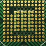
BGA via in pad technologies PCB prototype China,
Contract manufacturing of multilayer pcb, HDI PCB via in pad
via in pad high speed PCB /USA/UK/India/South Africa
via in pad |
|
via in pad BGA PCB Manufacturer, |
| BGA PCB |
|
High speed PCB |
| HDI PCB |
|
BGA via in pad technologies |
via in pad |
|
BGA via in pad technologies |
| BGA PCB |
|
High speed PCB |
| HDI PCB |
|
PCB prototype China, |
via in pad |
|
via in pad high speed PCB |
| BGA PCB |
|
Contract manufacturing of multilayer pcb, |
| HDI PCB |
|
via in pad BGA PCB Manufacturer, |
Vias in the pads in high speed PCB
-
Vias in the pads in high speed PCB
Vias in the pads are useful in high speed designs since they reduce trace length and therefore inductance (i.e. the connection goes straight from pad to plane rather than pad-trace-via-plane) You have to check whether your PCB house can do this though, and it may cost more (via will need to be plugged and plated over to provide a smooth surface) If you can't put the via in the pad, putting directly adjacent and using more than one can help reduce inductance.
They are also useful for Micro-BGA designs, where space is very limited and traditional fanout techniques cannot be used.
A via-in-pad (or capped/plated via) is not to be confused with a "tented via", which is a standard via with soldermask covering the hole (hence "tented")
To illustrate the advantage, here is an example of a TQFP footprint fanout with standard vias and via-in-pads:
It's easy to see why the via-in-pad version is preferable for high speed designs that need to keep inductance low.
The reason it's more expensive is due to the complex process (compared to standard vias) and potential problems (e.g. plating bulging with expansion of plug, or dimpling)
This document discusses various plugging techniques.
VIA IN PAD - WHY AND HOW
There are many reasons you shouldn’t use via in pad. It’s not good practice, and those via holes act like BGA via in padlittle capillary straws and suck solder off of the pad or the BGA.
That said there are some applications that may require, or seem to require, via in pad. Here are a few examples of why you might need to use via in pad:
If there is not enough space on the board.
It can help with thermal management.
Trace routing may be easier with via in pad.
High frequency designs benefit from the shortest possible routing to bypass capacitors, which may indicate via in pad.
So if you don't have a choice, here are some methods you can try when using via in pad:
Filled viasHave the board fab house plug the via and then plate copper over it. This is our favorite option. It will give you all of the benefits of via in pad without causing problems in assembly. It's really our only recommended via-in-pad method.
Via in Pads and BGA
-
Via in Pads and BGA
via-padsIn PCB design, via refers to a pad with a plated hole that connects copper tracks from one layer of the board to other layer(s). High-density multi-layer PCBs may have blind vias, which are visible only on one surface, or buried vias, which are visible on neither, normally referred to as micro vias. The advent and extensive use of finer pitch devices and requirements for smaller size PCBs creates new challenges. An exciting solution to these challenges uses a recent, but common PCB manufacturing technology with self descriptive name, “via in pad”.
Via in pad helps to reduce inductance, increase density and employ finer pitch array packages. The via in pad approach places a via directly under the device’s contact pads. This allows higher component density and improved routing. Consequently, via in pad provides the designer significant PCB space savings. For example, traditional fan-out places four components, whereas with via in pad, six components can be placed within the same board outline.
Filled via in pad is a way to achieve intermediate density with an intermediate cost compared to using blind/buried vias.
0.5 mm Pitch BGA Routing Solution
There is a reasonable solution for via fanout and a routing solution for the 0.5 mm pitch BGA but we need to think outside the box. The board thickness is an important factor because it affects the hole plating aspect ratio. If you use a 1 mm PCB thickness and want to achieve a 7:1 aspect ratio (this is common among all manufacturers) then the smallest hole size is 0.15 mm (6 mil). There are manufacturer’s that can hard drill a 0.15 mm (6 mil) hole through a 1 mm PCB. There are manufacturers that claim they can easily handle 10:1 aspect ratios. This means that they can drill 0.15 mm (6 mil) holes through 1.57 mm (0.062”) thick PCB material and plate the hole without problems. Drilling all the way through the PCB is important because sequential lamination is an expensive process.
For all via-in-land technology, a thermal relief on the voltage and ground plane connections must be used to prevent cold solder joints. A direct via-in-land connection to the plane will dissipate the heat required to melt the solder around the BGA ball and this will result in a cold or cracked solder joint. The exception to this rule is if the via only contacts a single plane with ½ OZ. copper or less.
What is Via in pad technology?
Connect via holes in solder pads is a big trouble in pcb assembly process.
Especially,when the via in BGA pads,
But the designer often based on its design can not achieved.
In fact,the electronic products is getting smaller,printed circuit board going to smaller,high density and more layers,so,many CAD Engineers( PCB Layout engineers) design the via in pads. in particular,small BGA ball space of BGA Pads,there is no enough place Could place the via holes.
It is disaster for SMT engineers.
With the improvement of via in pad technology, the solder problem can be solved.
Via in pad guidelines
1. plug via by solder mask.
This solution is suitable for big solder SMD pads, no cost addition.
The standard LPI solder mask process cannot tent of fill vias without the risk of exposed copper inside the hole barrel. typically,a secondary screen print operation is used that deposits uv or thermally curable epoxy soldermask into the holes to plug them.
This is called via plugging. Via plugging is used to plug via holes with a solerrsist material to prevent air leakage during in circuit test, or to prevent shortin from Components that are close to the board surface.
Via in Pad Technology
What is Via in Pad? In shortly,via in pad is the via holes are at the SMD pad.The vias are very small,usually under 0.3mm.Why and how? First is there is no enough space to layout,you have to put the vias and holes closer even together.Second it helps thermal management and for high frequency boards,it may help improve signals.
Because the SMD pads are for SMD components loading,so the solder can not flow to inner layer or the other side when assemble.That is the most important for via in pad board.
How PCB manufacturers like us to do via in pad board? We will fill all vias with non-conductive epoxy and plate copper over it ,so the vias are flat same as others. Many PCB factories are unable to do such capability.
The key technology is how we fill vias and guarantee there is no any solder (surface finishing) in the holes.
Filled via in pad is a way to achieve intermediate density with an intermediate cost compared to using blind/buried vias.
A Proper Approach to Via in Pad
-
A Proper Approach to Via in Pad
Via in pad seems to be one of the hot topics these days. It's a bit of a tough one too. The SMT guys pretty much always say: "don't ever do it." However, with certain parts, the component manufacturer strongly recommends it. You got to love those mutually exclusive requirements. Rather than just telling you "no, never," we’re going to do our best to give a few guidelines on how to do it properly.
We don't like it, but with some designs, if done properly, there can be a number of compelling reasons for putting vias directly in the SMT pads for BGA and QFN packaged components.
It can make routing easier with big or fine pitch BGAs
It can allow really close placement of bypass capacitors
It can help with thermal management
It can help with grounding on high-frequency parts.
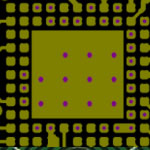
Via In Pad (Active Pad)
This process is becoming more and more common as BGA packages are becoming tighter. Rather than using the standard “dog bone” land pattern to transfer signal from the BGA footprint to a via that passes signal to other layers, vias can be drilled directly into the BGA footprint pads. This allows much simpler routing by soldering directly over the via. Make sure this process is called out in your fab notes.
TIP : We need to know the location, qty and size of the holes that need to be Via In Pad. The following steps are taken in this process.
Drill the via (thru hole or blind)
Fill the via with non-conductive material. Conductive material can be used but it’s not recommended since conductive material expands much more quickly than the surrounding laminate when heated which can cause cracks and pad failures during the assembly process.
The surface of the plugged via is then plated over with copper.
The newly plated copper surface is flattened and smoothed (planarized) to be even with the surrounding copper features.
The final finish is applied
You now have a solderable surface mount pad that also passes signal to inner layers eliminating the need to rout the signal to a via on the surface layer.
Via in PAD(VIP) PCB
In PCB design,via in pad (VIP) technology is widely used in small size PCBs with limits space for BGA.
the via in pad process allows vias to be plated and hidden beneath BGA pads. it required PCB manufacturer plugged the vias with epoxy and then plated copper over it,made it virtually invisible.
Via in pad PCB technology
Advantages with via in pad technology are:
Via in Pad can improved trace routing.
Via in PAD can help thermal dissipate.
Via in pad can help reduce inductance in high frequency board.
via in pad can provide a flat surface for component.
Via-In-Pad
This project explores whether PWB laser drilled micro-vias positioned in surface mount lands used for attachment of ball grid array components, have a negative impact on long term product reliability. Both plastic and ceramic ball grid arrays are included in the study.
Previous studies have indicated that, although the source of voids in ball grid array solder joints, laser drilled microvias have little impact on the performance of BGA interconnect reliability in accelerated thermal cycling (ATC). It has also been noted that SnPb ball grid array solder joints predominantly fail on the component substrate side and not at the ball to PWB interface, typically where the micro via induced void is PWB or component substrate interfaces. This raises the question of when failures do occur at the PWB side does the presence of a void accelerate this failure.
Void in BGA solder joint caused by outgassing of a microvia positioned in the centre of the attachment pad
For furhter information, please feel free to contact us, www.pcbsino.com

 English
 Español
 Português
 Deutsch
 Français
 Italiano
 Россия
 Türkçe
 Polski
 대한민국
대한민국
 بالعربية
 فارسی
فارسی
 Dutch
Dutch
 Afrikaans


