PCB edge plating with gold, side plating, PCB manufacturing, PCB prototype
half hole pcb, Mass Production, RF PCB,edge plating, side plating
High Frequency PCB,Shenzhen,China/USA/UK/India/South Africa
edge plating |
|
PCB edge plating PCB Manufacturer, |
| gold plating |
|
half hole PCB |
| gold shield |
|
PCB edge plating with gold, |
edge plating |
|
High Frequency PCB, |
| half hole |
|
RF PCB boards with edge shield |
| half hole |
|
RF PCB,edge plating |
edge plating |
|
RF PCB boards with edge shield, |
| edge shield |
|
RF PCB,edge plating |
| gold shield |
|
Carbon/Silver Ink Printing or Gold-plated Surface |
Feasibility of PCB edge plating?
-
Feasibility of PCB edge plating?
How feasible is it to edge plate a PCB or at least a portion of one? I've seen it done but as I understand the outer edge is only cut after plating at most fab houses. Is this something that's commonly possible? I'm currently working on a board that would benefit from this as it slides into a metallic case and needs to be connected to it.
The board on the radio product that I work on has its edges plated so that it makes contact with the metallised housing and screens. The most important thing to ensure is that your internal power planes do not come to the edge of the board and short to the edge plating.
During the manufacture the edges to be plated are cut by milling slots in the board material. I believe that these edges can then be plated at the same time as any plated through holes.
Edge Plating side plating PCBs
Circuit Board Castellations
Definition
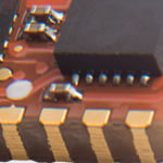
The industry generally accepts edge plating, or castellations, as copper plating that continues from the top and bottom surfaces and along one or more perimeter edges.
Applications for PCB Castellation
Edge plating and castellations are used in, but not limited to, edge soldering, edge connections, and current carrying capacity.
EDGE PLATING PCB / CASTELLATIONS DESCRIPTION:
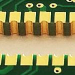
Edge Plating does not have a set definition per IPC. However, the industry generally accepts this as being copper plating that continues from the top and bottom surfaces and along one or more perimeter edges. Edge Plating can be used for a variety of purposes, including, but not limited to edge soldering, edge connections, and to increase current carrying capacity. Burrs Often edge plating, especially on castellations, can result in burrs from the final machining process.
We apply a modified, proprietary process flow that results in the burrs being polished down to the edge of the feature. Copper Peeling Plating over a large substrate surface can lead to the plated copper peeling due to a lack of adhesion strength. We address this by first roughening the surface through a combination of chemical and other proprietary means. We then use direct metallization, which has a higher copper bond strength, to prepare the surface for plating.
side Edge Plating PCB
-
Edge Plating PCB
In order to give an impression of the function of a shielding it is necessary to describe the electro-plating process. The production step of plating is an elementary one in PCB production. The galvano-technical connection of several layers in a PCB is done by a cathodic-anodic procedure for copper deposition at the inner wall of a drilled hole. In a topological sight the inner wall of a hole is part of the PCB surface.
The electro plating process therefore always causes a metallic deposition on the PCB surface. This surface can be modified in different ways by holes, slots or millings. If the subsequent PCB edge is to be metallised mainly minor logistic re-arrangement of production steps is necessary.
The edge to be plated isn’t processed (as usual) in one of the last production steps but has to be carried out already before the plating process.
To elaborate the contours milling tools are advisable. With these tools straight or rounded contours are produced without any problem. Cut-outs and/or partial milling of the contour is possible. Milling can be performed to open the contour over the complete thickness of the PCB. Anyhow, it is possible to have plated z-axis millings, opening the panel surface only down to a certain depth. If a plating of the complete outer contour of a PCB is desired it has to be considered that for the following production steps 1-2 mm wide pegs to hold the PCB within the panel are necessary which cannot be plated. The edges of all plated contour millings will have the same galvanic final surface plating as the actual PCB (see figure 1).
Manufacturing costs for plated edges are low.
Edge Plating (Edge Castellation) PCBs
The industry generally accepts edge plating, or castellations, as copper plating that continues from the top and bottom surfaces and along one or more perimeter edges.
The most common challenges to plated edges are preparing the edge surfaces so that the adhesion of the plated copper is adequate.
PCB Edge Plating
MCL offers a state-of-the-art printed circuit board fabrication facility, allowing us to overcome many problems common in the industry. This includes proper execution of PCB edge castellation, where we can keep quality to tight tolerances for edge plating, even after profiling.
You might have heard this concept called “edge plating” or “castellation,” which is the copper plating that runs from the top to the bottom surfaces of a PCB, and runs along at least one of the perimeter edges. PCB edge castellation ensures a strong connection through the board and limits the chance of equipment failures, especially in controlling protections for small form factor boards and sub-motherboards.
Edge Plating PCB Process
Circuit board fabrication for edge soldering requires precision handling and faces many challenges around how plated edges are prepared and the lifetime adhesion of the plated material. MCL has established industry practices and uses other optimum standards to ensure that our PCB edge castellation thoroughly prepares edge surfaces, applies the plated copper for immediate adhesion and processes the board to ensure long-term adhesion of every layer.
By using a controlled process in our circuit board fabrication for edge soldering, we can limit any potential hazard for through-holes and half-holes on the edge. The most significant concern is the creation of burrs, which will lead to the failure of mission-critical parts and can damage your equipment.
Applications
Edge plating circuit boards are common in many industries, and edge plating is a common practice. You’ll find PCB edge castellation (or edge plating PCB) applied in many cases, including:
Improving current-carrying capabilities
Edge connections and protection
Edge soldering to improve fabrication
Better support for connections such as boards that slide into metal casings
Edge Plating side plating(Castellation)
-
PCB Edge Plating (Castellation)
Definition
The industry generally accepts edge plating, or castellations, as copper plating that continues from the top and bottom surfaces and along one or more perimeter edges.
Applications
Edge plating and castellations are used in, but not limited to, edge soldering, edge connections, and current carrying capacity.
What are the advantages of Edge Plating PCB?
One speciality of the PCB for the application platform “meltemi” is edge plating (or edge metallizing). Edge plating provides clear measurable advantages at comparably ignorable costs for devices with moderate or high demands regarding EMC, signal-integrity and de-heating. Practice has proved that the theory can be implemented and works.
Regarding EMC aspects a device is operating stabile if it doesn’t radiate own interferences (emission) and doesn’t show any reaction to interferences being radiated by other devices (immission). In a technical view these interferences are caused by signal transmission between components of a device or between several parts or boards of a device system. Specific signal transmission in complex multilayer systems takes place via signal tracks on the PCB. Power supply is provided by plane areas or plane layers.
It has to be considered, that for each signal transmission a back current path has to be provided (the so-called GND plane) and that the transport of the information doesn’t take place in two-dimensional packets but three-dimensional electro-magnetic fields. Therefore any device (and any PCB) is a giant electronic microcosm with an hardly imaginable diversity of happenings in smallest spaces.
ALWAYS FOLLOW THIS README FILE. THE README IS LEADING OVER ANY FILLED IN FORM ON ANY WEBSITE
QUESTIONS CAN BE ASKED WITH MENTIONING THE FOLLOWING INFORMATION
PHNX Partnumber U251P 059 B
PCB name NRF210 RF
Designer cust.
Engineer VT
PRODUCT SPECIFICATION
Number of layers 4
Multi layers Top,Inner1, Inner2, Bottom
PCB material Copper top Copper inner 1" RO4350B 254um 2 layer boardmaterial. Copper 35um.
Copper 35um
Copper bottom Copper inner 2" RO4350B LoPro 526um 2 layer boardmaterial.
The two boards are attached to eachother with no flow prepreg.
Board Stackup file Top,Inner1, Inner2, Bottom
FR4 TG TG 130 140
Flammabilityrate UL 94 V O
PCB Thickness 1.0 ±0.1mm
Thickness copperlayers 1OZ/35um
Copper finish Immersion Gold
Edge Plating All edges and holes are side plated with gold.
min track/spacing 6/6mil
min hole size 0.3mm ±0.01mm
Goldfingers No
Soldermask Top Green
Soldermask Bot only bare visible gold. No silkscreen, no soldermask. But allowed in transport lines
Silkscreen Top White
Silkscreen Bot None
Vias VIP in SMT pads drawn in file
- "U251P 059 B NRF210 RF CopperTop CopperInner1"
- "U251P 059 B NRF210 RF CopperTop CopperBottom"
must be plugged and tented with copper.
PANELIZATION
Number of boards in panel 3 pcs
U251P 059 B NRF210 RF README
Panelization 1 x 3
PCB dimension 68.0 x 108.0 mm
Panel dimensions 224.0 x 128.0 mm
Board separation methode Internal routing with break tabs with and stamp holes According drawing file U251P 059 B NRF210 RF Panelization.gbr
De paneling milling and breaktabs
Internal milling No internal milling
Tooling holes Allowed in the conveying edges.
X Out boards in panels Allowed, maximum of 1pcs cross out boards in a panel
Cross out boards do not count toward the total requested PCBs.
X Out boards should be packed separate
REMARKS
Copper top contents gold plated copper (immersion gold), Silkscreen, soldermask. Copper bottom contents only bare visible gold. No silkscreen, no soldermask.
Tooling Holes Tooling holes in conveying/technical edges of the panel are allowed.
Shielding holes It is allowed to increase the distance between the shielding holes (diam. 0.15mm) on the boardedges to prevent drilling problems.
X Out boards Allowed for 10%
X Out boards do not count toward the total requested PCBs. X Out boards should be packed separate
For furhter information, please feel free to contact us, www.pcbsino.com
 English
 Español
 Português
 Deutsch
 Français
 Italiano
 Россия
 Türkçe
 Polski
 대한민국
대한민국
 بالعربية
 فارسی
فارسی
 Dutch
Dutch
 Afrikaans


