Multilayer PCB Prototype Manufacturer China,impedance control HDI
Contract manufacturing of multilayer pcb, blind/buried via,Mass Production
Multilayre PCB, High speed,Shenzhen,China/USA/UK/India/South Africa
multilayer pcb is useful in high-speed application
-
multilayer pcb is used very normal.
The multilayer pcb is mainly used in industry electronic equipment,Like computers and military equipment, especially in the case that need light weight and volume.The multilayer pcb is also useful in high-speed application. The mltilayer pcb can provide more space for the conductor pattern and power.
Multilayer PCB |
|
Multilayer PCB Prototype |
| blind via |
|
Manufacturer China,impedance control HDI |
| HDI PCB |
|
blind/buried via,Mass Production |
Multilayer PCB |
|
blind/buried via,Mass Production |
| HDI PCB |
|
impedance control HDI |
| blind via |
|
Medical equipment aplication |
HDI PCB |
|
impedance control HDI |
| impedance |
|
0.1mm Laser drill via |
| Laser drill |
|
Multilayer PCB Fabrication |
Multilayer PCB |
|
Multilayer PCB Fabrication |
| impedance |
|
Multilayer PCB Prototype |
| Laser drill |
|
Carbon/Silver Ink Printing or Gold-plated Surface |
impedance |
|
Multilayer PCB Fabrication |
| Multilayer PCB |
|
Multilayer PCB Prototype |
| Aplication: |
|
Industry control boards |
Benefits of Multilayer PCBs
-
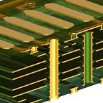
The multilayer pcb is made up by more than two layers which are stacked together with reliable through via or blind via between them. There are at least three conductive layers in one multilayer pcb with two layers outside and the one layer inside the PCB. Due to the complex manufacturing process and lower production , the cost of multilayer pcb is relatively higher.PCBSINO is specialized in multilayer PCB manufacturing for many years.
Benefits of Multilayer PCBs
Benefits of Multilayer PCBs (compared to single or double-sided PCBs)
Higher assembly density
Smaller size (considerable savings on space)
Increased flexibility
Easier incorporation controlled impedance features. EMI shielding through careful placement of power and ground layers.
Reduces the need for interconnection wiring harnesses (reduces overall weight)
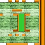
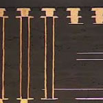
multilayer PCB fabrication – lay-up and bond
The outer layers of our multilayer consist of sheets of glass cloth pre-impregnated with uncured epoxy resin (prepreg) and a thin copper foil.
for 6layer blind via 5days fast prototype:
1) PCB layers: 6
2) Impedance control: yes, details specified on GM2
3) Electrical test: Yes,
4) Dimensions: 119.5x149.5mm = 180 sq cm
5) Minimum hole size: 0.2mm
6) Minimum Track/Clearance: 5mil/5mil
7) Solder mask: Green on both sides
8) Silkscreen: white on both sides
9) Outer copper: 1 Oz.
10 Inner copper: 1 Oz.
11) IPC level: III
12) Panel: 2 designs
13) Board cut: CNC routing/ Vcut, outline specified on GM3
14: Quantity:112
15) PCB finish: ENIG
16) Layer stack: specified on GM2, or closest available.
17) Smallest component size: 0402
The assembly information is also provided.
for 16layer blind via PCB
3. Manufacturing class/accuracy:
Minimum clearance 0,12 mm;
Minimum trace width 0,075 mm;
Minimum plated via size 0,2х0,4 mm;
with bind buried vias.
4. Layers – 16
5. Material – Rogers4003C Rogers4350B and Fr-4 Tg170 mixed core,
The laminated materials are 106 (FR-4), 1080 (FR-4).
6. Total board thickness – 1.6 mm
7. Copper thickness – all layers 18 um
8. Layer structure filename
layer name:
1. .GTL — Top Layer
2. .GP1 — Ground Plane 1 (inverse)
3. .G1 — PWR1
4. .G2 — PWR2
5. .GP2 — Ground Plane 2 (inverse)
6. .G3 — L1
7. .GP3 — Ground Plane 3 (inverse)
8. .G4 — L2
9. .GP4 — Ground Plane 4 (inverse)
10. .G5 — L3
11. .GP5 — Ground Plane 5 (inverse)
12. .G6 — L4
13. .GP6 — Ground Plane 6 (inverse)
14. .G7 — L5
15. .GP7 — Ground Plane 7 (inverse)
16. .GBL — Bottom Layer
.GTO — Top Overlay
.GTP — Top Paste
.GTS — Top Solder (inverse)
.GBS — Bottom Solder (inverse)
.GBP — Bottom Paste
.GBO — Bottom Overlay
.GPB — Bottom Pad Master
.GPT — Top Pad Master
.GKO — Keep-Out Layer
.GM4 — Mechanical 4 (Board shape outline)
9. Drill pair – ‘Top-L2, L15-Bottom’ (through via and blind buried via.)
Vias are solder mask tented (layers .GTS, .GBS).
Filled and Capped Vias IPC4761 Type VII.
10. Soldermask color - Green
11. Silkscreen color
White - .GTO Top Overlay
White - .GBO Bottom Overlay
12. Hole structure filenames
13. Surface finish
Lamel edge connector - hard gold (galvanic)
All other part of pcb - Immersion gold ENIG
14. Board shape processing - Milling
15. Automated PCB Assembly
16. Impedance control - needed
a) Differential pairs
100Ω
width / space
0.1 / 0.12 mm
Layers: Top (GTL), G3(L1), G4(L2), G5(L3), G6(L4), G7(L5), Bottom (GBL).
b) Single ended traces
50Ω
width 0.13mm - Layers: Top (GTL), Bottom (GBL).
width 0.075mm - Layers: G3(L1), G4(L2), G5(L3), G6(L4), G7(L5).
17. Board Size
with craft edges = 180.61 х 97.7 mm
without craft edges = 180.6 х 73.7 mm
18. Chamfering for Card-edge connector (Lamel) according to attached pdf.
19. Testing
AOI – 100% pass
BGA X-Ray Inspection – 100% pass
Electrical test – 100% pass
Package requirement – Vacuum, moisture-proof, anti-deformation, anti-scratch
Impedance report – needed
Test report – needed
Quality guarantee – needed
20. PCB stackup ( Altium Designer )
for 12layer blind via PCB prototype
Item Description and requirements
Acceptance criteria IPC Inspection standard document (see Appendix 1)
PCB Layer 12
Drill pair Via1-2,Via2-3,Via3-10,Via10-11,Via11-12,Via1-12
Impedance Control 50ohm 100 ohm(+/-10%)
Dimension (+/-0.15 mm)
V-CUT
Total thickness 1.2 mm (-10%MM)
material The default core material is FR-4,The default layering material is RCC;If can meeting the product
performance, the laminated material also can used 106(FR-4)、1080(FR-4)and LDPP.
Surface finish ENIG
if microvia electroplated filled? No
Soldermask plug via 1. 1. both side with soldermask, then plug via with soldermask
3. 2. If via Both side open window, don't plug via with soldermask.
5. 3. one side with soldermask, the other side open window, then plug via with soldermask.
7. 4. One side is covered with soldermask, the other side is half open-window via, Make plug via. but accept 2mil (max)exposed copper (gold ring) on plug via position. if via to open-window pad distance less than 3mil, then plug via.The vias less than 3mil from the PAD position of the window shall be plugged, but 2mil (max)exposed copper (gold ring) on plug via position can be accepted.
Nickel thickness 2.54-6 um
Gold thickness 0.03-0.1 um
Hole copper thickness Through hole 20um,Single point 18um;Blind via 12um,Single point 10um;Buried via 15um,Single point 13um
Inner layer Oxide
Surface layer thickness 25 um(min)
Soldermask material Taiyo
Soldermask thickness Trace edge soldermask thickness Min.5um, upon copper surface is 10-50um
Silkscreen color white
NC-drill tolerance NPTH tolerance +/-2mil;PTH tolerance +/-3mil; microvia after electroplating 0-0.1mm
Trace tolerance +/-1mil(for trace width smaller than 5mil), the others tolerance +/-20%.
Pad tolerance +/-1.2mil(for BGA pad), the other pad tolerance +/-20%.
AOI AOI 100% pass
Electrical test Electrical test 100% pass
Reliability test Thermal shock and weldability
other Microsection and impedance test report
Board warpage ≤0.7%
Company Logo accept
Stencil file Gerber Files
Package requirment Vacuum, moisture-proof, anti-deformation, anti-scratch
Multilayer PCB
Multilayer PCBs have one or more conductor pattern inside the board, to increase the area available for the wiring. This is achieved by gluing (PP) many double-sided circuit boards together with insulating layers in between.
The number of layers is referred to as the number of separate conductor patterns – usually including the two outer layers. Most boards have between 4 and 8 layers, but PCBs with almost 100 layers can be made.
Since the layers in a PCB are laminated together, it’s very difficult to tell how many there are, but if you inspect the side of the board with magnifier closely you might be able to count them.
Large super computers often contain boards with multilayer PCB.
Applications of Multilayer PCBs
-
Applications of Multilayer PCBs
While the weight and space benefits of multilayer PCBs are especially valuable for Aerospace PCBs, multilayer PCBs are also apply to many critical product. below are a few other the applications using multilayer printed circuit boards:
Computers
File servers
Data storage
Signal transmission
Cell phone transmission
Cell phone repeaters
GPS technology
Industrial controls
Satellite systems
Hand held devices
Test equipment
X-ray equipment
Heart monitors
Cat scan technology
Atomic accelerators
Central fire alarm systems
Fiber optic receptors
Nuclear detection systems
Space probe equipment
Weather analysis
PCBSINO specializes in manufacturing high-difficulty PCBs with advanced technology and strict quality control, catering to the most demanding applications in automotive, medical, industrial control, and high-frequency communication fields. Our high-difficulty PCBs cover a full range of complex processes, including high-layer count multilayer PCBs (up to 40 layers), HDI PCBs with first and second order blind & buried vias, strict impedance control PCBs, heavy copper PCBs, high Tg PCBs, rigid-flex PCBs, and special material PCBs such as Rogers PCB. We have rich experience in fast prototyping and mass production of high-difficulty PCBs, adhering to ISO 9001 and AS9100 certifications to ensure each product meets international standards. With professional R&D team and advanced production equipment, we provide one-stop customized solutions for high-difficulty PCB manufacturing, from design optimization, material selection to assembly service, helping customers achieve product upgrading and technological breakthroughs.
For furhter information, please feel free to contact us, www.pcbsino.com
 English
 Español
 Português
 Deutsch
 Français
 Italiano
 Россия
 Türkçe
 Polski
 대한민국
대한민국
 بالعربية
 فارسی
فارسی
 Dutch
Dutch
 Afrikaans