Highly reliable Al2O3 Ceramic PCB aplication
Highly reliable Al2O3 Ceramic PCB aplication
-
Highly reliable Al2O3 Ceramic PCB aplication
Ceramic PCBs boast better overall quality, higher resolution, and excellent bonding properties over organic, rendering the substrate more conducive to producing precision patterns, and providing better protection from moisture ingress.
Further space savings over Surface Mount Technology and Chip-On-Board
Alumina (AL2O3), Aluminum Nitride (AlN), and Beryllia (BeO) base material available
Very compact with low profile and low mass
Provides reliable performance in extreme temperature operating range
Superior Base Material Power Dissipation
Alumina (AL2O3) High Level ~ 1 Watt per inch per degree C
Aluminum Nitride (AIN) Higher Level ~ 7 Watts per inch per degree C
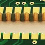
Why Ceramic PCB has such excellent performance? You can have a brief view on its basic structure and then you will understand.
96% or 98% Alumina (Al2O3), Aluminum Nitride (AIN), or Beryllium Oxide (BeO)
Conductors material: For thin, thick film technology, it'll be silver palladium (AgPd), gold pllladium (AuPd); For DCB (Direct Copper Bonded) it'll be copper only
Printed thick film resistors range in value from 0.1 ohm to 300 megohm
Temperature Coefficient Resistance (TCR) as low as 50 ppm with tracking TCR's to 20 ppm
Power ratings range one-sixteenth (1/16) to five (5) Watts
Automated Laser Trimming of Resistors
Precision Resistors to one-tenth of one percent (0.1%)
Ratio Matching to one-tenth of one percent (0.1%)
Epoxy and eutectic semi-conductor die attach
Though the benefits of ceramic printed circuit boards are many, the drawbacks should be considered:
This ceramic material is characterized by its extremely high strength and thermal conductivity. The outstanding surface quality on both sides makes it the perfect companion for any commercial thick film paste and even makes it suitable for a number of thin film applications (sputtering).
Rubalit® 710 with 99.6% Al2O3
Welcome to P.W. Circuits LTD a UK Design, Manufacturing and Assembler of Printed Circuit Boards. From our site in Leicester we support a wide product range of high technology PCBs for the military, medical, aerospace, telecoms and other industries. We specialise in all areas of PCB production, the design of a new board and the manufacture & assembly of prototype or small to medium size batches of PCBs. With over 40 years experience in the PCB industry we will work with you to meet your requirement in technology, delivery and cost.
The advantages with using us as a "one shop stop" for your PCB Manufacture and Assembly is immediately apparent; a cost effective, single source manufacturing solution for your business, no 'passing the buck', all your data is safe as we manufacture your board here in our factory, no need for multiple NDA's, just one small invoice at the end and a quality PCB for your product.
We manufacture a vast range of pcb's with our expertise covering simple single sided boards through to high count flexi-rigid multilayer boards. We have a large experience handling many different types of materials from Ceramic (Alumina) to PTFE and everything in between.
Please explore our extensive website and if you have any questions then please don't hesitate to contact us, you can call, email, live chat or Skype us and one of our dedicated engineers will be able to help you with your enquiry.
Thick film materials are most widely used in screen printing electronic circuits. The thick film paste can be printed on various substrates such as ceramic, metal or glass. A typical thick film paste has conductive, resistive, or insulative properties which are chosen depending on the end application. During the screen printing process, thick film pastes are dried to evaporate the lower vaporization solvents at temperatures less than 150°C. The printed thick film layer then enters a high-temperature firing step (500°C – 1,100°C) to sinter and form a bond to the substrate. Firing results in a dense body which acts as a signal controller (conductors or resistors) or isolator (dielectric or overglaze). This process can be repeated multiple times, alternating a conductive layer and a dielectric layer, to create a multilayer thick film circuit.
with HASL Surface Finish
Inquire Now
Min. Order: 1 Square Meter
FOB Price: US$ 70 - 75 / Square Meter
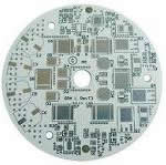
Ceramic PCBS 2layers HAL Lead Free
Thick Film technology is ideally suited when quick turnaround is required for complex, high density multi-layer, low cost, high volume applications. It is also extremely effective for development work, quite often surpassing PCB turnaround. The ability to print resistors, capacitors, and inductors on ceramic based substrates allows for increased package density and reliability.
Thick Film Technology has the advantages of circuit miniaturization together with increased reliability, low weight and Low cost. By using a Thick Film circuit instead of a PCB many benefits are gained – reduced component count, lower assembly costs, and quicker assembly/test times along with increased reliability. The characteristics of Thick Film Technology make it highly applicable to Commercial, Industrial, Scientific and Military applications.
Thick Film Technology achieves this with the ability to produce integrated resistors of small size, planar 2D construction, with high reliability, high power density and high stability. This means that resistors can be made as small as 1mm square with no significant thickness. Components can be mounted on top of resistors to save space. Reliability is high since the resistors are integrated into the supporting substrate (ceramic) along with the terminations and conductor lines; hence there are no solder joints to fail under harsh conditions. Another added bonus is that the resistors are not limited to preferred values. Almost any value is possible from less than 1Ω to greater than 100 MΩ with tolerances as tight as 0.1% depending on value. The temperature stability is also very good with 100ppm/deg C being typical.
We can provide ceramic PCB for Russia customer for testing products. Why our customer want to use ceramic substrate to make pcb is that ceramic pcb are in high pressure, high insulation, high frequency, high temperature, and high reliable and minor volume electronic products
Why Ceramic PCB has such excellent performance ? the following is the highlights for your reference.
96% or 98% Alumina , Aluminum Nitride (AIN), or Beryllium Oxide (BeO)
Conductors material: For thin, thick film technology, it'll be silver palladium,gold platinum; For DCB (Direct Copper Bonded) it'll be copper
Application temp: -55~850C
Thermal conductivity value: 24W~28W/m-K (; 150W~240W/m-K for AIN , 220~250W/m-K for BeO;
Max compression strength: >7,000 N/cm2
Miniature components
A wide range of miniature components in various forms can be assembled onto a Thick Film circuit to make a Thick Film Hybrid Circuit. These components can be unpacked silicon circuits to packed surface mount components. Conductive epoxy, eutectic and Solder attachment methods may be used. It is possible to combine these methods on one circuit.
Inquire Now
Min. Order: 1 Square Meter
FOB Price: US$ 300 - 302 / Square Meter
2-layer Ceramic PCB
In the power electronics world, Direct Bonded Copper (DBC) is the primary substrate technology. In this paper, we will discuss an alternative technology utilizing screen printable copper pastes (Thick Printed Copper - TPC) on a variety of substrate technologies including Alumina (Al2O3) and Aluminum Nitride (AlN). These materials when
processed, look and perform similar to DBC, but exhibit superior reliability and excellent design flexibility. DBC has drawbacks when it comes to thermal mechanical reliability and lacks the flexibility to have multiple copper thicknesses for power and signal circuits within the same design, which is easily achieved via screen printing. The benefits of this TPC system will be demonstrated through data generated on passive thermal shock tests in comparison to high end DBC. Furthermore, this Thick Print Copper technology has the excellent potential for replacing high end Metal Core Printed Circuit Board (MCPCB) technology due to utilization of higher thermal conductive dielectric materials like Al2O3 and AlN. This will allow for designers to drive their LED's harder and effectively producing LED modules with higher power densities.
Inquire Now
Min. Order: 1 Square Meter
FOB Price: US$ 1 / Square Meter
Freight Cost Available
C-MAC is one of the pioneers in thick film technology and started screen printing in 1965. As a standard 96% Al2O3 (known as alumina) substrates in different thickness and size are used, but alternatives like AlN or metal are possible. Conductors are made of Ag, Au, Pt, Pd and alloys of these metals.
C-MAC offers a broad range of technical options like metallized through holes, multilayer, fine line, thick silver, printed resistors etc. The highly automated production lines are installed in a clean room and can handle volumes from a few hundred to millions per year.
Thick film technology is known for its high reliability and stability, excellent power handling, high packing density and high temperature capability. It is well suited for the integration of analogue, digital and power electronics on the same substrate.
Electrical circuit layers including conductors and insulators are printed automatically on a ceramic substrate and fired in special furnaces. The printed resistor’s electrical resistance and the substrate’s shape are customised to the module requirements by laser trimming and scribing.
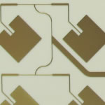
Figure 1: Typical steps followed to achieve multiple thicknesses on the same substrate through the use of TPC thick film materials and standard screen printing processes. Thru-hole connections can be made for the option of two-sided boards via stencil printing a compatible high viscosity, copper, thru-hole thick film material.
Circuits built using Thick Print Copper (TPC) technology provide a more reliable alternative to DBC, Direct Plated Copper (DPC), or MCPCB substrate technologies for high power applications. As with standard thick film materials, the copper paste is screen printed on the substrate and dried at 125°C for 10 minutes; followed by firing at 900°C – 925°C in a nitrogen-blanketed muffled furnace. Through repeating the above steps, fired-film thicknesses up to 300 microns can be achieved. By varying the screen design on different layers, multiple thicknesses can be achieved for different parts of the circuit (Figure 1).
To create a circuit layer, DBC and MCPCB use copper foils at a specific thickness. The layer thickness is constant across the entire substrate and cannot be easily varied. For DPC, the copper layer thickness is built up through the plating process to one consistent circuit layer thickness across the entire substrate. With TPC, the copper thickness on a circuit can be varied easily by screen printing. Each layer is individually added, allowing for varying thicknesses by selective deposition, as illustrated in Figure 1.
The versatility of TPC provides design engineers with more flexibility and quicker design optimization. TPC substrates utilize the same assembly materials that DBC, DPC and MCPCB use including Pb-free solders, conductive epoxies, wire-bonding materials (Au, Al, and Cu), ribbon-bonding materials (Al and Cu), and silver sinter materials with very little optimization needed.
Longer durableness Al2O3 Alumina ceramic polished substrates
US $0.5-1 / Piece
100 Pieces (Min. Order)
Qinhuangdao Fulianjing Electronics Co., Ltd.
Thin Film/Alumina/Al2O3/Ceramic Dbc Substrate
US $1-500 / Piece
1 Piece (Min. Order)
Yaspro Electronics (Shanghai) Co., Ltd.
While it is well known that LEDs chips are efficient in converting electrical energy to light energy as compared to others (and are expected to be more efficient in the future as scientists are working new chip designs, materials and processes), there remains a large fraction of electrical energy is lost as heat.1 Removal of this heat from the chip to ambient has been a challenge for the LED packaging industry.2 The mechanism of heat dissipation in LEDs is totally different from that observed in incandescent lamps and CFLs. For example, the filament temperature in an incandescent lamp is ~2500C, while the typical LED chip junction temperature is below 125C. In incandescent lamps, a significant amount of unwanted heat generated is dissipated as infra-red (IR) radiation while heat transfer by radiative process in LEDs is negligible. The primary mode of heat dissipation in LED is conduction through the substrate. Therefore, the LED packaging and assembly industry had to find creative ways to find a low resistance heat conduction path from LED to ambient. This led to development of new packaging materials including the sub-mounts/substrates, circuit boards and materials used to join these parts. This study investigates the impact of substrate materials on long-term reliability of high power LEDs.
View Specs
Industrial Adhesives - Electrically Conductive, Silver Epoxy -- EPO-TEK® E3001
Supplier: Epoxy Technology
Description: paddle, COB, advanced packages, and hybrid circuits. o Hybrid Microelectronics: die attach bonding onto ceramic PCB, as well as attaching SMDs onto the same substrate. o Opto-electronics: �� Die attach of LEDs, LED arrays, LED on PCB, or packaged onto lead-frames.
Substrate / Material Compatibility: Metal, Plastic
Industry: Electronics, Semiconductors / IC Packaging
Chemical / Polymer System Type: Epoxy (EP)
Filled / Reinforced: true
Supplier Catalog
Go To Website
Download
Datasheet
View Specs
Polymers and Plastic Resins - Spectrally Transparent Epoxy -- EPO-TEK® 301
Supplier: Epoxy Technology
Description: wafer passivation, solder mask and flex circuits; compatible with LED die, Si, GaAs. • PCB: general potting and protection over FR4, flex, or ceramic PCBs. • Medical: o It is NONTOXIC—complying with USP Class VI Biocompatibility standards. Suggested for medical
Material Type / Grade: Thermoset
Chemical / Polymer System Type: Epoxy
Filler Material: Unfilled
Resins & Compounds: Liquid
Supplier Catalog
Go To Website
Download
Datasheet
View Specs
Industrial Valves - TitanEZ™ Manifold Mount Without PCB no stator -- EZ011-020
Supplier: IDEX Health & Science
Description: Our TitanEZ Manifold Mount w/PCB and Stator valve has a small footprint and is capable of millions of actuations due to the ceramic-on-ceramic dynamic surfaces. It is a 10-position, 11-port motorized selector valve intended for manifold mounting. This model comes with a
Valve Type: Directional Valves
Primary Material of Construction: Other
Valve Size: 0.0625 to 0.1250 inch
Number of Ports/Ways: 11
Traditionally, LED dies are mounted on an Al2O3 or AlN sub-mount using a die attach material. Then this LED package is assembled with solder materials on a circuit board. In a new emerging packaging process, LED die are directly attached on a circuit board through a chip-on-board (COB) process. In both packaging schemes, the circuit board technologies, in addition to its primary role of providing a mechanical fixture and path for electrical connections, also provide a route for heat dissipation from LED die to the heat sink. Therefore, appropriate
selection of the circuit board material is of utmost importance as the total thermal resistance of the whole stack should be as low as possible (provide ref). Materials with poor thermal conductivity can result in fast degradation of the LED due to high temperature operation at high power.3 Operating the LED at lower current to maximize efficiency, limits the total light output from the LED.
Ceramic Substrates (DBC)
200 Pieces (Min. Order)
XELLATECH PTE LTD
With its extremely fine surface quality, this ceramic material is designed especially to meet the highest demands in thin-film technology.
Rubalit® 708 HP – High Performance with 96% Al2O3
Rubalit® 708 HP offers consistently reliable and convincing performance even when subject to high thermal and electrical loads in terms of its:
Thermocycling capability
Thermal shock resistance
Flexural strength
Surface quality
Thermal conductivity
This makes Rubalit® 708 HP ideal for power electronics in conjunction with direct copper bonding (DCB) and active metal brazing (AMB).
The cost difference is substantial. The decision to print on a ceramic substrate will require an initial investment up to 10 times higher than to print on an organic one.
The technology is still relatively new, and so few printed circuit board manufacturers are offering the capability to build on and with the ceramic substrate.
Decided an organic printed circuit board is right for your application?
Where the manufacturing of a ceramic PCB requires a punching process, an organic substrate is manipulated using an organic solderability preservative (OSP), a method for coating of printed circuit boards. This water-based organic compound selectively bonds to copper and protects the copper until soldering.
An organic substrate enables the printed circuit board manufacturer to employ an additive screen process instead of an edge-removal, etched process—the end result, a PCB design that is nearly entirely organic.
Express PCB |
|
Rigid PCB Rapid Prototype,24 hours |
| Fr4 PCB |
|
prototype Lower to 15USD ! |
| Rapid Prototype |
|
Fr4 Rigid PCB Rapid Prototype China, |
MCPCB |
|
MCPCB Manufacturer China, Shenzhen |
| Aluminum PCB: |
|
Aluminum Metal Core PCB manufacturing, Fabrication |
| Aluminum PCB: |
|
single side, double side MCPCB, 0.5-5mm or more |
Rogers 4350B |
|
Rogers 4350,Rogers 4003 Manufacturing |
| Rogers 4350B |
|
Rogers 4350B,4003C PCB Manufacturer |
| Ro4350B |
|
Rogers High Frequency PCB Manufaturing China |
Turnkey Services |
|
Turnkey PCB Assembly Services, |
| Turnkey services |
|
Print circuit board Manufacturing, Turnkey Services |
| Turnkey Assembly |
|
Through Hole PCB components wave soldering Assembly |
For furhter information, please feel free to contact us, www.pcbsino.com