Development with Direction : From Concept to Launch PCBSINO Designer provides businesses with the tools, manpower and expertise needed to turn a great product idea into a successful product ready to ship.
LEDs, Wifi, Bluetooth, and NFC modules, sensors, HD displays, cameras, and more to work together seamlessly. We have successfully completed projects featuring battery technology, solar power, X-ray systems, virtual reality (VR) tech and more.
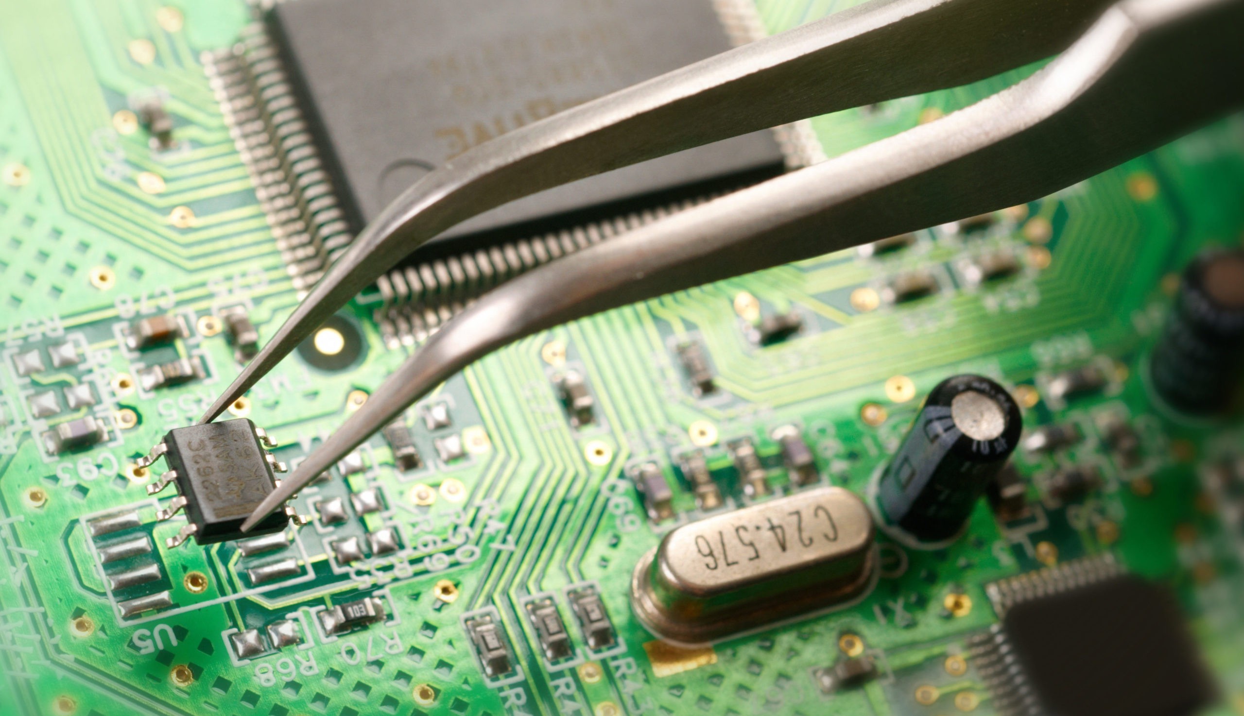
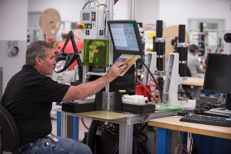
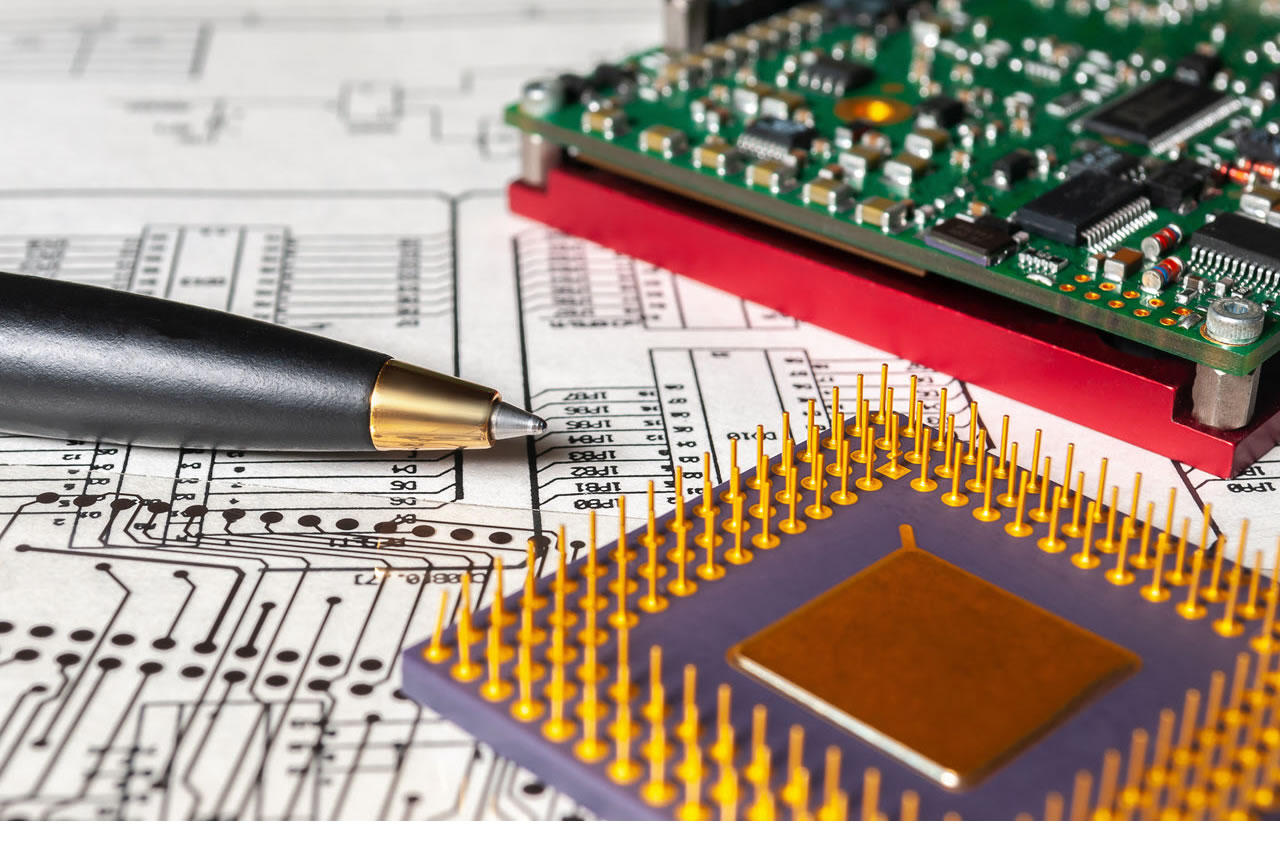
PCBSINO has over 30 years of deep domain expertise in schematic capture, layout, validation, test, and other areas of microelectronic design. With an extensive library of circuitries, layout stack-ups, modular test infrastructure and other re-usable hardware blocks, we can efficiently design complex and exceptionally reliable embedded hardware.
With decades of design and manufacturing experience, leverage our expertise at any point in your project to accelerate time to market.
Gerber Files Drill Files Rout data for PCB cutouts BOM, including unit and 1,000 piece parts cost. Pick and Place file (centroid data) for automated assembly.
Offload your carrier board design to PCBSINO Engineering to receive first article prototypes quickly and reduce risk by leveraging our knowledge of the System on Module to accelerate schematic capture, PCB layout, and design verification.
For furhter information, please feel free to contact us, www.pcbsino.com

The Expertise to Work as an Extension of your Team
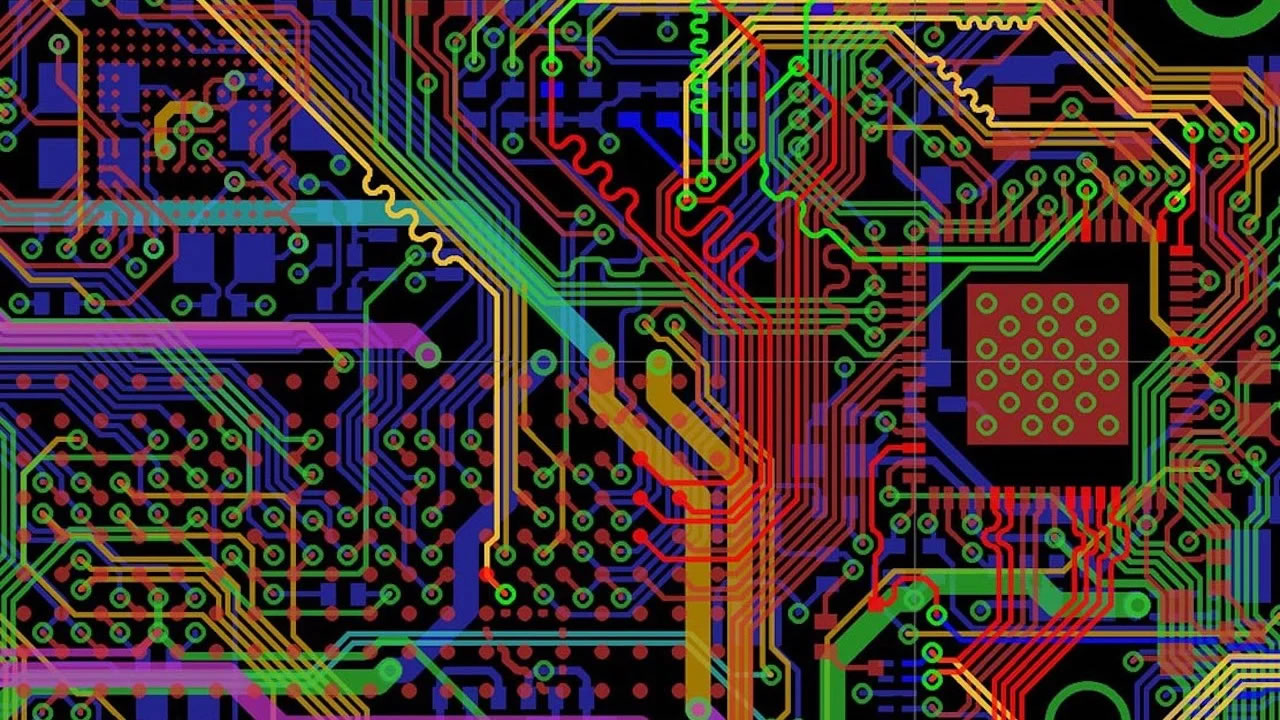
PCB layout
Mixed speed and signal technology
High-speed digital and analog design
Low EMI/RFI design
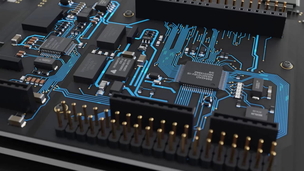
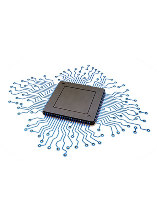
μBGA, dual-die, fine pitch, PoP (package-on-package), microvias PCB technology, passive components as small as 01005 inch (0402 metric) packaging
Power rail separation, Power over Hours (PoH) analysis
High-density, multi-layer (12+), small form factor PCBs
Signal integrity analysis
Advanced simulation, 3D modeling and pre-compliance testing
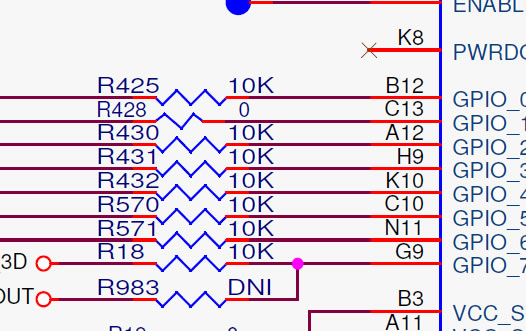
We can take your schematic in any form (pdf, sketch, etc.) and convert it into a proper electronic CAD format. We will create Cadence // PADs // Altium schematic symbols and PCB footprints for each part in your design.
Deliverables:
Complete Electronic Project File including:
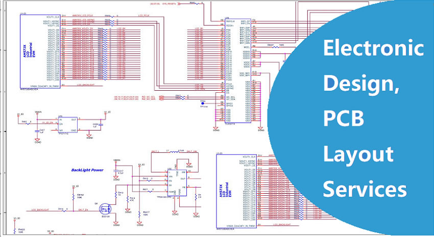
Schematics
PCB Layout
Output Settings File
DFM (Design for Manufacturing) Checks ...
 English
 Español
 Português
 Deutsch
 Français
 Italiano
 Россия
 Türkçe
 Polski
 Suid-Afrika
 بالعربية
 فارسی
فارسی


