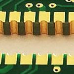
High Frequency Al2O3 Ceramic PCB aplication
China PCB Manufacturing, Shenzhen PCB Manufacturer, Making Circuit boards
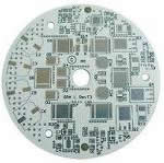
PCB Contract manufacturer, PCB Fabrication, Turnkey assembly services
Buy Print circuit board, customer: /USA/UK/Canada/South Africa...
PCB Supplier Shenzhen, China, PCB Manufacturer, Turnkey services
-
PCBSINO is the Top 5 PCB manufacturer company in China.
PCBSINO do rapid Prototype within 24 hours. our rigid PCB like MCPCB and Rogers PCB, FR4, High TG FR4, Rogers 4003, 4350,Al Aluminum metal Core MCPCB, Al2O3 Ceramic,Taconic,Halogen Free material, CEM-3, Fr2, CEM-1, CEM-2, 94VO, Rogers HF material, Polymide, etc.
PCBSINO making many type electronic product for our customer, Our turkey services team can source original components part for your project(Digikey/Mouser/RS...), senior Electronic engineer will follow each step of the production to solve any PCB problem and our team will do final function test in PCB house.
Express PCB |
|
Rigid PCB Rapid Prototype,24 hours |
| Fr4 PCB |
|
prototype Lower to 15USD ! |
| Rapid Prototype |
|
Fr4 Rigid PCB Rapid Prototype China, |
MCPCB |
|
MCPCB Manufacturer China, Shenzhen |
| Aluminum PCB: |
|
Aluminum Metal Core PCB manufacturing, Fabrication |
| Aluminum PCB: |
|
single side, double side MCPCB, 0.5-5mm or more |
Rogers 4350B |
|
Rogers 4350,Rogers 4003 Manufacturing |
| Rogers 4350B |
|
Rogers 4350B,4003C PCB Manufacturer |
| Ro4350B |
|
Rogers High Frequency PCB Manufaturing China |
Turnkey Services |
|
Turnkey PCB Assembly Services, |
| Turnkey services |
|
Print circuit board Manufacturing, Turnkey Services |
| Turnkey Assembly |
|
Through Hole PCB components wave soldering Assembly |
High Frequency Al2O3 Ceramic PCB aplication
-
High Frequency Al2O3 Ceramic PCB aplication
Higher operating temperature up to 350ºC
Lower expansion coefficient (6-8 ppm/ºC)
Good thermal properties (22-24 W/mK)
Superior high-frequency performance
Smaller package size due to integration and multi-layer possibilities
Cost effective for dense package due to parallel processing of layers
Hermetic packages possible, 0% water absorption
Good light reflection due to white color.
Limited to no outgassing
Strong rigid material
Ceramic Printed circuit board (Ceramic PCB) includes Alumina (Al2O3), Aluminum Nitride (AIN) with high pressure, high insulation, high frequency, high temperature, and high reliable and minor volume electronic products, so Ceramic PCB will be your best choice.
Why Ceramic PCB has such excellent performance? You can have a brief view on its basic structure and then you will understand.
96% or 98% Alumina (Al2O3), Aluminum Nitride (AIN), or Beryllium Oxide (BeO)
Conductors material: For thin, thick film technology, it'll be silver palladium (AgPd), gold pllladium (AuPd); For DCB (Direct Copper Bonded) it'll be copper only
Application temp: -55~850C
Thermal conductivity value: 24W~28W/m-K (Al2O3); 150W~240W/m-K for AIN , 220~250W/m-K for BeO;
Max compression strength: >7,000 N/cm2
Breakdown Voltage (KV/mm): 15/20/28 for 25mm/0.63mm/1.0mm respectively
Thermal expansion conefficient(ppm/K): 7.4 (under 50~200C)
Our Ceramic PCB capability:
DK Thermal manufacturers Alumina Oxide (Al2O3) 96% by using both thick film process as well as direct bonded copper (DBC) / Direct Plated Copper Technologies (DPC) to print the circuits.
Circuits can either be printed using Copper (Cu) or Silver (Ag) depending on the application and the request. Copper is offered both in DBC/DPC as well as Thick film screen print processes while silver can only be done in using second manufacturing option. We advise copper in 1-2 layer applications from low to high volume applications. Silver is advised when going to multi-layer and only in medium to high volume due to the higher tooling costs. In case you are unsure what material to specify, please to not hesitate to contact us.
Packing: Inner anti-static bag + outer exporting standard carton.
Aluminum Oxide (Al2O3)
Aluminum Oxide is the standard microelectronic substrate material for the vast majority of applications. Although it has low thermal conductivity - it has excellent mechanical and electrical properties and is used in DC to High Frequency applications. Al2O3 is available in standard 96% grade for low cost, and general electronics 99.6% for higher frequency applications. Aluminum Oxide is the first and only choice for many designers.
Benefits of Aluminum Oxide (Al2O3) ceramic substrates
High mechanical strength
Low Thermal Conductivity
Good Dielectric properties
Excellent high temperature characteristics
Excellent metalizing properties for thick film, thin film, and DBCu
Excellent electrical insulation
Good corrosion and wear resistance
Available in As-Fired, Lapped, and Polished ceramic substrates
Material specifications (PDF)
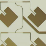
DBC (Direct Bonding Chips) Ceramic + copper foil circuits board
DBC heat-sinking substrate for solar battery is fabricated
by using bonding technology under high temperature.
The conjunction between copper foils and ceramic is molecular
bond and any adhesion agent is not being used.
Due to the fine adhesion between copper foils and ceramic plate.
it can suffer from strict thermal cycling test. under the normal
temperature environment,the islation performance and material
strength can hold several hundred thousand hours stability.
Other materials can not compare to this on.
Because the ceramic material has fine thermal conductive preperty
the compound material has low resistance.
In the succeeding processes,by the photoresist and
Chemical etching methods and fine laster cutting process.
DBC heat-sinking substrate for solar battery possesses various accurate
and complex patterns and outlines.
Advantage:
1. High thermal conductivity property and low thermal resistance,
Could increase the efficiency and operation lifetime of semi-conductor chips
2. Excellent thermal cycling performance and fine mechanic strength.
3.High isolating strength
4.The thermal expansion coefficient is close to that of the silicon chip.
5.Strong current conductive ability
6.Fine environment compatiblity,no environment contaminative elements,
such as PB,Hg and Cr,etc.
Be able to pass strict environment protection credentials.
Download Ceramics_PCB_introduce
As a special pcb manufacturer ,Andwin be able to make all type ceramic pcb for customer!
Sample of Ceramic PCB:
Why Choose Us?
1. Quality
Our UL/Rohs standards insure high-quality pcb assemblies from start to finish. No matter it's a simple custom PCBA or a complex turnkey production run, RayMing will adhere to the highest quality standards.
HTFC called high temperature fused ceramic substrate, high temperature insulation and heat conduction of the AL2O3 or AIN ceramic substrate using single or double plate, printing technology, printing materials will Gao Chuandao into line, sintering sintering furnace is placed in the 850~950 degrees C, can be completed
LTCC(Low-Temperature Co-fired Ceramic)
LTCC also known as LTCC substrates, this technology must first be inorganic alumina powder and more 30%~50% glass material with organic binder, the mixed slurry is called mud installed, then use the scraper to scrape the slurry into sheets, followed by a drying process of sheet forming a slurry thin pieces of embryo, and then according to the design of each layer of the drill holes, as each layer of transmission signal, inside LTCC using screen printing technology, respectively in the embryo on pore filling and printed circuit, and electrode can use silver, copper, gold and other metals, the layer laminated action, sintering sintering furnace is placed in the 850~900 degrees C, can be completed.
HTCC(Hight-Temperature Co-fired Ceramic)
LTCC Also known as low temperature co-firing multilayer ceramic substrate, the technology must be will inorganic alumina powder with the first 30% ~ 50% In the glass Materials with organic binder, The mixing called for mud pack size, Then use the scraper scraping paste flakes. again Through a drying process will flake pulp formed thin pieces of embryo, Then according to the design of each layer drill guide hole, As each The signal transmission, LTCC Internal wiring with screen printing technology, born in embryo do fill in the hole and printed circuit, inside The outside electrode can be respectively used silver, copper, gold and other metals, finally will do laminated layers, placed in 850 ~ 900 ° C The burning Knot in the furnace sintering molding, can be completed
DBC(Direct Bonded Copper)
DBC is directly connected to the copper substrate, the high insulation of AL2O3 or AIN ceramic substrate coated with single or double copper metal after heating by high temperature environment, 1065~1085 ~ C, the copper metal because of high temperature oxidation, and the spread of AL2O3 material (Eutectic) Eutectic melt, copper metal ceramic substrate adhesion, shape ceramic composite metal substrate, according to circuit design, etching line with.
DPC(Direct Plate Copper)
DPC also known as direct copper substrate, the ceramic substrate pretreatment cleaning, using thin film manufacturing technology - vacuum coating on ceramic substrate sputtering on copper metal composite layer, and then coated with a photoresist photolithography exposure, developing, etching, to film process to complete the line, and finally to plating / electroless deposition increase line thickness, to resist removal after completion of metal production line.
Metal package are the preferred package choice for high heat dissipation, high component count & density such as Multi–chip–module(MCM) and critical EMI shielding applications. Metal package can be designed to fit custom application at low volume with reasonable tooling cost. Ceramic Package, on the other hand, provides a small footprint and fine I/O pitch package solution. Ceramic package can be designed for ultra high temperature applications starting at 500°C. Tooling cost is typically much higher than metal package. Ceramic package is suitable for medium to high volume applications. It is absolutely the choice of the end users to select the right kind of package for their particular applications. Both metal and ceramic packages can be sealed hermetically.
Microelectronic circuits and components that are exposed to harsh environments require hermetic packaging. Beyond providing mechanical protection and thermal dissipation, a hermetic package prevents the intrusion of atmospheric contaminants such as moisture, ionic contaminants, airborne particles and unwanted gases.
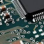
High-precision multi-layer circuit boards and high difficult pcb with special treatments are the core products of Witgain. For high difficult pcb with special treatments, our products mainly cover the following kinds:
1)thick copper pcb: the thickest copper for double layer is 28OZ, for inner layer in multi-layer is 15OZ, for out layer in multi-layer is 28OZ
2)rigid-flex pcb: from double layer to 16 layer
3)thick gold pcb: the thickest gold is 140U'
4)metal basement pcb: AL basement pcb, Copper basement pcb, Iron basement pcb
5)Ceramic pcb: AL2O3
6)High-frequency pcb: Rogers series, Arlon series, Isola series
7)Hybrid: Rogers+FR4 Hybrid pcb
8)AL+PI FPC
9) Back pcb: up to 40 layer
10)HDI PCB: 3+N+3
11)Others: Via on pad, horn hole and so on
This article provides an overview of some of the critical materials issues involved in the utilization and commercialization of aluminum-nitride ceramics in electronic applications. Critical material defects and microstructural issues that control thermal, electrical, and mechanical properties and the status of metallization technology are reviewed. Finally, a discussion of current and future potential applications of sintered AlN and how these applications tie into key material properties is provided.
Thermal conductivity value: 24W~28W/m-K (Al2O3); 150W~240W/m-K for AIN , 220~250W/m-K for BeO;
Max compression strength: >7,000 N/cm2
Breakdown Voltage (KV/mm): 15/20/28 for 0.25mm/0.63mm/1.0mm respectively
Thermal expansion conefficient(ppm/K): 7.4 (under 50~200C
HITECH CIRCUITS CO.,LIMITED provides full service with single and double-sided ceramics PCB and substrates manufacturing. The technology is developed and patented by Hitechpcb company. Company know-how allow to manufacture high quality ceramics substrates and PCB on Al2O3 and AlN materials. The key advantages are in precision patterns, high-quality processing, excellent solderability and bond ability with single- and double-side metalized ceramics processing.
HITECH CIRCUITS CO.,LIMITED patented technology provides significant advantages over typical thin- and thick-film metallization processes. Single and double-sided ceramics PCBs have better quality, higher resolution, high conductivity, excellent solderability and bonding properties.
We provide fast development and manufacturing of metallized ceramics substrates and ceramics PCBs for LED applications, optoelectronics industry, high-frequency PCB for Telecommunication and other applications.
The main application for these substrates is the manufacturing of electrical circuits on one or two faces for such various fields as :
the automotive and consumable goods
industrial sensors
medical equipment
airborne microelectronics devices for the aerospace and defense.
Products
Microcertec offers customized substrates manufactured by Accumet Engineering Corporation in terms of thickness, flatness and roughness. Depending on customers' application we can offer :
lapped substrates in 96 % alumina for thick-film metallized circuits
polished substrates in fine-grain 99,6 % alumina for thin-film metalized circuits to be used in low to medium power RF and microwave devices
aluminium nitride substrates that can be lapped or polished depending upon the metallization process for use in high-power RF and microwave devices
fused silica substrates for high-frequency thin-film metallized circuits requiring low loss performance
sapphire substrates that require optimum thermal dissipation.
2. Experience
Established in 2005, we have more than 10 years’ experience in PCB manufacturing and PCB Assemblies with good knowledge in this field.
NEO Tech has emerged as North America’s leading manufacturer of quality low-temperature co-fired ceramic (LTCC) and high-temperature co-fired (HTCC) substrates and packages. These fabrication technologies provide unique solutions for high interconnect density, compact networks and high-frequency applications. Our ceramic substrate facilities also produce both thin and thick film parts for a wide variety of OEMs in medical, telecommunications, and defense markets.
3. Protecting your interests
High Temperature Electronic Packaging (–55°C to 250°C)
RF Electrical Design
Substrate and PCB Layout Design for HI–REL applications
Custom Metal and Ceramic (HTCC, LTCC) Package Design
Multi–layer Thick–Film Substrate Fabrication (Al2O3, AlN, BeO)
Hybrid Microcircuit Assembly and Test in Class 10K clean room environment
CSP, Flip Chip & BGA Component Mounting
Hermetic Package Sealing for HI–REL applications (Projection, Seam and Cold welds)
Bare Die Procurement and Handling
Quartz BAW Resonator Design & Fabrication (Round, Strip and HFF Inverted Mesa configurations)
SAW Wafer Fabrication in Class 100 clean room environment
Wafer deep etching technology for Wafer Level Packaging
Process and Test Equipment Design
Environmental MIL–PRF Screening
Custom Process Equipment Design
Physical Design Modeling and Finite Element Analysis
All Docs and Files from your side are kept confidential under our control for protecting your intellectual property.
Tensky ceramic PCB is made up of innovative, research and development engineers the configuration, the target is the first leader professional Ceramic base plate, ceramic circuit board brought to workshop, using a semiconductor membrane technology for a customer with OEM/ODM service, Resolution, Customer in electronic circuit in various thermal heating, high pressure, and the problem.
Main materials:Al2O3 and AlN substrate.
Image layers metal:Ti, TiW, Cu , Ni, Pd , Au , Ag, AuSn, Sn, Al…and other metallize。
Primary market:high-power LED stand, cooling, optical communication components, optical power solar energy base plate, vehicle with electrical, air, and the electronic circuit board roadbed, and so on.
The special is high power LED market context, such as 1515, 2016, 3535, 5050, 6060, 1215 substrate, and LED - COB integrated stand, practices, as well as UVLED stand, etc. product is the Secretary's main work specifications, provide customer professional views, reduced customer test and failure risk.
Specification:OEM/ODM
Size:OEM/ODM
Introduction:Ceramic circuit board has a resistance to high voltage, high current, fast heat dissipation, high thermal
Ceramic circuit board has a resistance to high voltage, high current, fast heat dissipation, high thermal stability characteristics, such as the semiconductor industry, optical industry and mainframe devices, fiber-pass design, high-frequency communications, LED industry, solar industry, IC packaging, car electronic circuits, electronic circuit applications such as military maturing and growth.
Introduction:
RUSALOX was established in December 2010 in order to organize the mass production of high thermal conductivity elements based on al oxide technology. The company was started with the participation of RUSNANO, venture capital fund ‘Tamir Fishman CIG’ and Russian Venture Company. In August 2011 RUSALOX signed long-term lease contracts of production, office space and equipment with OJSC ‘Vladimir Production Association’. In September 2011 RUSALOX started producing and selling al oxide PCB using the leased equipment.
The launch of the first manufacturing line with a capacity of 200 panels (~ 6.000 sq.dm) per month took place in February 2012. In December 2013 the second manufacturing line with a capacity of 400 panels (~ 12.000 sq.dm) per month was launched. The first export sales were made already in a year – at the end of 2014. At the end of 2015 the total revenue from the sales of al oxide products increased by 2.1 times in comparison to 2014. Since the end of 2015 RUSALOX is exporting its al oxide products to the international markets – Europe and Asia.
This section ceramic circuit board design concept is a dedicated supply LED module plant, can be directly packaged
chips directly Wire bonding brighter and longer life on the system board, because the ceramic heat with excellent
results, but also allow your LED
Any interest, please feel check following contact info:
Sales Manager:
NEO Tech also provides next generation Etch Conductor Photolithography (ECP) Thick Film Substrates suitable for microwave and high-resolution lines and space applications. The Thick Film conductor material is fired in a dense, non-porous film over a large area of the substrate. The high resolution lines are then defined using photoresist and etch techniques to achieve widths and spaces as low as 0.003″ (0.0762mm). The ECP process is based around standard thick film Au that is already qualified by many OEMs, thus avoiding long qualification cycles and bringing customers to market quickly. ECP technology allows designers to combine RF and digital functions on substrates, and offers options for integrating capacitors, resistors, inductors, couplers, and filters. Capacitors and resistors can be laser trimmed to obtain +/-3% and +/-1% tolerances, respectively.
High frequency applications through 100 GHz
Etched conductors [0.001” (0.0254 mm)] lines/spaces
Precision layer to layer dielectric alignment (+/- 12.5 micron) in multilayer construction
Dense, solid thru-holes [0.007” (0.178 mm diameter)] for interconnection/grounding
On-circuit integration of passive components including Lange couplers, resistors (0.5 Ohm – 100 m Ohm, trimmed to 1%) and capacitors (5 – 200pF, trimmed to 3%), inductors, couplers, and filters.
30% to 50% lower insertion loss
For furhter information, please feel free to contact us, www.pcbsino.com