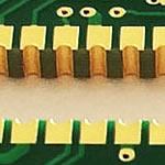
High voltage Al2O3 Ceramic PCB aplication
China PCB Manufacturing, Shenzhen PCB Manufacturer, Making Circuit boards
PCB Contract manufacturer, PCB Fabrication, Turnkey assembly services
Buy Print circuit board, customer: /USA/UK/Canada/South Africa...
PCB Supplier Shenzhen, China, PCB Manufacturer, Turnkey services
-
PCBSINO is the Top 5 PCB manufacturer company in China.
PCBSINO do rapid Prototype within 24 hours. our rigid PCB like MCPCB and Rogers PCB, FR4, High TG FR4, Rogers 4003, 4350,Al Aluminum metal Core MCPCB, Al2O3 Ceramic,Taconic,Halogen Free material, CEM-3, Fr2, CEM-1, CEM-2, 94VO, Rogers HF material, Polymide, etc.
PCBSINO making many type electronic product for our customer, Our turkey services team can source original components part for your project(Digikey/Mouser/RS...), senior Electronic engineer will follow each step of the production to solve any PCB problem and our team will do final function test in PCB house.
Express PCB |
|
Rigid PCB Rapid Prototype,24 hours |
| Fr4 PCB |
|
prototype Lower to 15USD ! |
| Rapid Prototype |
|
Fr4 Rigid PCB Rapid Prototype China, |
MCPCB |
|
MCPCB Manufacturer China, Shenzhen |
| Aluminum PCB: |
|
Aluminum Metal Core PCB manufacturing, Fabrication |
| Aluminum PCB: |
|
single side, double side MCPCB, 0.5-5mm or more |
Rogers 4350B |
|
Rogers 4350,Rogers 4003 Manufacturing |
| Rogers 4350B |
|
Rogers 4350B,4003C PCB Manufacturer |
| Ro4350B |
|
Rogers High Frequency PCB Manufaturing China |
Turnkey Services |
|
Turnkey PCB Assembly Services, |
| Turnkey services |
|
Print circuit board Manufacturing, Turnkey Services |
| Turnkey Assembly |
|
Through Hole PCB components wave soldering Assembly |
High voltage Al2O3 Ceramic PCB aplication
-
High voltage Al2O3 Ceramic PCB aplication
The high heat conductivity as well as the high heat capacity and thermal spreading of the thick copper cladding makes curamik substrates indispensable to power electronics. The mechanical stress on silicon chips mounted directly on the substrate (Chip on Board) is very low, since the coefficient of thermal expansion (CTE) of the ceramic substrate is better matched to the CTE of silicon compared to substrates using a metal or a plastic basis
curamik substrates are produced in a master card format of 5“x7“ and 5,5“x7,5“. The individual parts can be left in the master card format to support more efficient assembly and mounting of components before being separated into individual pieces. We also offer single pieces for single piece assembly.
Aluminum Oxide, Al2O3 Ceramic Properties
Alumina is one of the most cost effective and widely used material in the family of engineering ceramics. The raw materials from which this high performance technical grade ceramic is made are readily available and reasonably priced, resulting in good value for the cost in fabricated alumina shapes. With an excellent combination of properties and an attractive price, it is no surprise that fine grain technical grade alumina has a very wide range of applications.
.Key Properties
Hard, wear-resistant
Excellent dielectric properties from DC to GHz frequencies
Resists strong acid and alkali attack at elevated temperatures
Good thermal conductivity
Excellent size and shape capability
High strength and stiffness
Available in purity ranges from 94%, an easily metallizable composition, to 99.8% for the most demanding high temperature applications.
.
Apart from MCPCB, if you want to use PCB in high pressure, high insulation, high frequency, high temperature, and high reliable and minor volume electronic products, then Ceramic PCB will be your best choice.
Why Ceramic PCB has such excellent performance? You can have a brief view on its basic structure and then you will understand.
The types of ceramic pcb substrates:
high temperature fusion ceramic substrate (HTFC)
low temperature co-fired multilayer ceramic (LTCC)
high temperature co-fired multilayer ceramic (HTCC)
direct bonding copper substrate (DBC)
Direct Copper Plating (DPC)
if you want to use PCB in high pressure, high insulation, high frequency, high temperature, and high reliable and minor volume electronic products, then Ceramic PCB will be your best choice.
This product is composed of a noble metal consisting of high-conductivity dielectric circuit and high thermal conductivity of insulating material combination of high thermal conductivity substrate. Can effectively solve the problem of low thermal conductivity of PCB and aluminum plate. To effectively heat the heat generated by the electronic components derived to increase component stability and extend the service life.
Why Ceramic PCB has such excellent performance? You can have a brief view on its basic structure and then you will understand.
96% or 98% Alumina (Al2O3), Aluminum Nitride (AIN), or Beryllium Oxide (BeO)
Conductors material: For thin, thick film technology, it'll be silver palladium (AgPd), gold pllladium (AuPd); For DCB (Direct Copper Bonded) it'll be copper only
Application temp: -55~850C
Thermal conductivity value: 24W~28W/m-K (Al2O3); 150W~240W/m-K for AIN , 220~250W/m-K for BeO;
Max compression strength: >7,000 N/cm2
Breakdown Voltage (KV/mm): 15/20/28 for 0.25mm/0.63mm/1.0mm respectively
Thermal expansion conefficient(ppm/K): 7.4 (under 50~200C)
Ceramic pcb is also a branch of the printed circuit board, ceramic substrate and CEM material substrate, FR-4 substrate is parallel, the production process is same, but the support material is not the same, so there is no substitute circuit board argument.
Now more than 90% of the market are FR-4 materials, the proportion of ceramic substrate is relatively small, and will not become mainstream.
96% or 98% Alumina (Al2O3), Aluminum Nitride (AIN), or Beryllium Oxide (BeO)
Conductors material: For thin, thick film technology, it'll be silver palladium (AgPd), gold pllladium (AuPd); For DCB (Direct Copper Bonded) it'll be copper only
Application temp: -55~850C
Thermal conductivity value: 24W~28W/m-K (Al2O3); 150W~240W/m-K for AIN , 220~250W/m-K for BeO;
Max compression strength: >7,000 N/cm2
Breakdown Voltage (KV/mm): 15/20/28 for 0.25mm/0.63mm/1.0mm respectively
Thermal expansion conefficient(ppm/K): 7.4 (under 50~200C)
Click here to see more details about ceramic substrate.
The inception voltage of a stack is nearly two times higher than that of a single Al2O3 ceramic with the same total thickness. Even the inception voltage of a Si3N4 ceramic is 1kV lower than that of the Al2O3 stack with the same total thickness. This is an effect of the homogenized electric fields.
Due to the high inception voltage it is possible to realize 4.5kV modules with an Al2O3 assembly which is impossible with today’s single layer substrates.
In a phase resolved partial discharge chart of the Al2O3 stack the PD events happen around 270°. This gives a hint on the PD mechanism. It indicates a coronary discharge normally caused by metallic edges at the border between potting material and ceramic layer. In a following insulation measurement a flashover occurred at 15kV from metallization edge through the potting material. The ceramic did not show any alteration. Even at this high voltage the Al2O3 stack with 0.32mm thick ceramic layers was not the limiting factor but the potting material or irregularities in the joint between potting material and ceramic like delaminations or voids in combination with high electric fields at sharp metallic edges. It should be mentioned that voids were not visible even under a microscope.
The investigations were repeated with a stack made of two 1mm thick AlN ceramics. PD started between 9-10kV and quenched at 8-9kV. The weak point could be found again in the combination of potting material and metal edges.
Conclusion
Simulations show that stacking two substrates in high voltage modules can significantly reduce the peak electric fields that are generated at sharp edges of the metal layers of these ceramics. Equal recess of the metal layers and doubling the middle and lower layer in thickness results in a reasonable homogenization of the electric field. The use of a third ceramic layer just causes a small benefit compared to the dual layer solution.
Stacking allows cheaper isolation solutions by replacing today’s Si3N4 or AlN substrate materials by Al2O3. These stacks are suitable for applications up to 4.5kV fulfilling both insulation and partial discharge requirements.
According to different manufacturing method, current there're three basic types for ceramic board:
■Good smoothness / flatness with less porosity. Excellent in adhesion with thin film and thick film materials.
■Less variance in outline, plate thickness, slit pitch, etc.
■Minimal warpage, bending, and undulation.
■Physical and chemical properties are stable even under a hot environment. Excellent in thermal shock resistance. High thermal conductivity and coefficient of thermal expansion similar to that of silicon.
■Superior mechanical strength. Products with higher mechanical strength are also in our lineup.
■Excellent resistance against oil and chemical.
■Excellent in insulation properties, high dielectric breakdown voltage, high surface resistivity / volume resistivity, and small dielectric constant.
■Stable breaking strength, and less variance in shape or dimensions.
■The high reflective substrate, especially suitable for optical applications such as LED, is also available.
Typical Uses
Gas laser tubes
Wear pads
Seal rings
High temperature electrical insulators
High voltage insulators
Furnace liner tubes
Thread and wire guides
Electronic substrates
Ballistic armor
Abrasion resistant tube and elbow liners
Thermometry sensors
Laboratory instrument tubes and sample holders
Instrumentation parts for thermal property test machines
Grinding media
General Information
The Nanotherm process converts the surface of a sheet of aluminium into a dielectric nanoceramic layer, with the crystals formed as small as 30 nanometres. As a conversion process is used to form the nanoceramic from aluminium it creates a robust bond between the dielectric and the base plate, resulting in a dense, uniform layer of ceramic which acts as a perfect dielectric.
The nanoceramic dielectric layer is usually between 10 and 30 microns thick, depending on the breakdown voltage required. This makes the thermal path between the LED chip and the aluminium as small as is feasibly possible, resulting in extremely high overall thermal conductivity and low thermal resistance.
There are two approaches to attaching the copper wiring trace to the nanoceramic. The most cost effective solution is to add a laminated copper surface – Nanotherm LC. For the most thermally demanding applications the copper layer is sputtered or plated on – Nanotherm DM, a fully inorganic MCPCB.
Aluminum oxide, commonly referred to as alumina, possesses strong ionic interatomic bonding giving rise to it’s desirable material characteristics. It can exist in several crystalline phases which all revert to the most stable hexagonal alpha phase at elevated temperatures. This is the phase of particular interest for structural applications and the material available from Accuratus.
Alpha phase alumina is the strongest and stiffest of the oxide ceramics. Its high hardness, excellent dielectric properties, refractoriness and good thermal properties make it the material of choice for a wide range of applications.
RMT Ltd provides full service with single and double-sided ceramics PCB and substrates manufacturing. The technology is developed and patented by RMT Ltd company. Company know-how allow to manufacture high quality ceramics substrates and PCB on Al2O3 and AlN materials. The key advantages are in precision patterns, high-quality processing, excellent solderability and bondability with single- and double-side metallized ceramics processing.
Primary market:high-power LED stand, cooling, optical communication components, optical power solar energy base plate, vehicle with electrical, air, and the electronic circuit board roadbed, and so on.
The special is high power LED market context, such as substrate, and LED - COB integrated stand, practices, as well as UVLED stand, etc. product is the Secretary's main work specifications, provide customer professional views, reduced customer test and failure risk.
The paper presents the study of the particle size distribution, surface area and their effect
on sintering of alumina (Al2O3) using additives such as magnesium oxide (MgO) and silica (SiO2),
so that the samples could be sintered to high relative density (~ 97.43 %) with controlled grain
growth. However, the use of MgO along with SiO2 on Al2O3 produced the powder compacts
having high Green density, sintered density with minimum porosity to achieve high dielectric
strength ceramic material, so that material can be used for high-voltage insulator applications.
Ceramic materials used in DBC include:
• Alumina (Al2O3), which is widely used because of its low cost and good thermal conductivity (24 W/mK).
• Aluminum nitride (AlN), which is more expensive, but has a better thermal performance (> 170 W/mK).
The coefficient of thermal expansion of Al2O3 (7.1 ppm/K) and AlN (4.7 ppm/K) is close to that of silicon (4 ppm/K). Therefore, DBC is suitable for robust packaging of bare dice since such assemblies will have a long product life. The layout is customized in a way similar to PCB. Special features to enhance the thermal cycling performance can be applied.
C-MAC is specialized in the fabrication of power assemblies based on DBC substrates. It offers a state-of-the art highly automated production process including 3D solder inspection, pick & place of components and bare dice, vacuum reflow with and without flux, AOI/AXI, cleaning, wire bonding and electrical test.
1. High Performance Printed Circuit Boards By Joseph Y. Lee Samsung Electro-Mechanics
2. Chapter - 4Advanced Ceramic Substrates for Microelectronic Systems
3. Desired Substrate Properties High electrical resistivity High thermal conductivity Resistance to temperature Inert to chemical corrosion Cost
4. Selected CeramicsTable 4.1 Melting Point of Selected CeramicsMaterial Melting Point °CSiC 2700BN 2732AlN 2232BeO 2570Al3O2 2000
5. Substrate Fabrication Roll compaction; large parallel rollers to form sheet. Tape casting; moving belt that flows under a knife edge. Powder pressing; powder into hard die cavity with high pressure through sintering process. Isostatic powder pressing; flexible die surrounded with water or glycerin and pressed up to 10,000 lb/in2 Extrusion; forced through a die. Very economical and produces thinner part.
6. Definitions Surface roughness; measure of the surface microstructure Camber; measure of the deviation from flatness (red line). deviation
7. Substrates Rules: Thicker substrates – less camber Squares are better than rectangles Pressed methods are better.
8. Thermal Properties Thermal conductivity (W/m-°C): q = -k (dT/dx) Specific heat (W-s/g-°C): c = dQ/dT Temp. coeff. of expansion (ppm/°C): α= [L 2) – L 1)] /[L 1)(T –T)] (T (T (T 2 1
9. Mechanical Properties Modulus of elasticity: E = TCE * ∆T Modulus of rapture (MPa): σ = Mx/I This can be used to measure tensile strength of thinned Si wafers. Maximum stress at the tip of crack: SM = 2 So < (a / ρt)0.5 Ratio of max. stress to applied stress: Kt = SM/S0 = 2 (a / ρt)0.5 Plain strain fracture toughness: KIC = Z Sc (pi * a)0.5 Critical force to cause breakage: Sc = KIC / [Z (pi * a)0.5]
10. Electrical Properties Resistivity: ρ= (1/σ) (Ω.cm) Current Density: J = σ E (A/cm2) Breakdown Voltage: (Volt) Dielectrics constant: ε (ratio) r Dielectric loss: tan(δ)
11. Metallization of Ceramic Substrates Thick film – additive process by which conductive, resistive, and dielectric patterns in the form of a viscous paste are screen printed, dried, and fired onto a ceramic substrate at an elevated temperature to promote adhesion of the film Thin film – subtractive process such that entire substrate is coated with several layers of metallization and unwanted material is etched away in a succession of selective photoetching processes. Copper 1) Direct bond copper 2) Plated copper 3) Active metal braze
You have a project or you just want to receive more information on our "Direct Bond Copper Assembly", please contact ou
Specification:OEM/ODM
Size:OEM/ODM
Introduction:Ceramic circuit board has a resistance to high voltage, high current, fast heat dissipation, high thermal
rO2 toughened A ceramic layers with required thickness were prepared by electrophoretic deposition (EPD) method using ethanol suspensions with stabilizing agent of polyethyleneimine (PEI) under constant-voltage mode in this paper. The deposition of Al2O3/ZrO2 ceramic powders occurred on the titanium alloy cathode. A stable suspension with 1wt% PEI in ethanol at pH 5 was prepared in terms of the zeta potential and sedimentation of the suspension. The effects of the suspension concentration, applied voltage, deposition time and processing method of titanium alloy cathode on the coating thickness and morphology were investigated. The deposition layers on titanium alloys with smooth surfaces and thickness of 0.35–1.2 mm could be obtained by adjusting the aforementioned parameters. In addition, after being sintered at 1500°C for 3 h in air atmosphere, ZrO2 toughened Al2O3 ceramic layers became smooth and dense.
Ceramic circuit board has a resistance to high voltage, high current, fast heat dissipation, high thermal stability characteristics, such as the semiconductor industry, optical industry and mainframe devices, fiber-pass design, high-frequency communications, LED industry, solar industry, IC packaging, car electronic circuits, electronic circuit applications such as military maturing and growth.
96% or 98% Alumina (Al2O3), Aluminum Nitride (AIN), or Beryllium Oxide (BeO)
Conductors material: For thin, thick film technology, it'll be silver palladium (AgPd), gold pllladium (AuPd); For DCB (Direct Copper Bonded) it'll be copper only
Application temp: -55~850C
Thermal conductivity value: 24W~28W/m-K (Al2O3); 150W~240W/m-K for AIN , 220~250W/m-K for BeO;
Max compression strength: >7,000 N/cm2
Breakdown Voltage (KV/mm): 15/20/28 for 25mm/0.63mm/1.0mm respectively
Thermal expansion conefficient(ppm/K): 7.4 (under 50~200C)
Our Ceramic PCB capability:
Introduction:
This section ceramic circuit board design concept is a dedicated supply LED module plant, can be directly packaged
chips directly Wire bonding brighter and longer life on the system board, because the ceramic heat with excellent
results, but also allow your LED
RMT patented technology provides significant advantages over typical thin- and thick-film metallization processes. Single and double-sided ceramics PCBs have better quality, higher resolution, high conductivity, excellent solderability and bonding properties.
High purity alumina is usable in both oxidizing and reducing atmospheres to °C. Weight loss in vacuum ranges from 10–7 to 10–6 g/cm2.sec over a temperature range of 1700° to 2000°C. It resists attack by all gases except wet fluorine and is resistant to all common reagents except hydrofluoric acid and phosphoric acid. Elevated temperature attack occurs in the presence of alkali metal vapors particularly at lower purity levels.
[1] S.T.Aruna, V.Ezhil Selvi, V.K.Wiliam Grips, K.S. Rajam: Corrosion and wear resistance properties of Ni-Acomposite coatings containing various forms of alumina, J.Appl. Electrochem.
Web of ScienceCrossrefGoogle Scholar
[2] S.T. Aruna, C.N. Bindu, V. Ezhil Selvi, V.K. William Grips, K.S. Rajam: Synthesis and properties of electrodeposited Ni/ ceria nanocomposite coatings, Surface & Coatings Technology
Google Scholar
[3] M. Karaś, M. Nowak, M. Opyrchał, M. Bigaj, A. Najder, Archives of Metallurgy and Materials,
Google Scholar
[4] Cullity B.D., Podstawy dyfrakcji promieni rentgenowskich, PWN, Warszawa 1964.
Google Scholar
[5] Neff H., Grundlagen und Anwendung der Röntgenfeinstrukturanalyse, Oldenbourg-Verlag, 2. Auflage
Google Scholar
[6] Warren B.E., X-Ray Diffraction. Addison-Wesley,
Google Scholar
Advantages:
Great heat conductivity and temperature resistance
High insolation voltage
High heat spread
Adjusted expansion coefficient enables chip on board
Efficient processing of master cards
For furhter information, please feel free to contact us, www.pcbsino.com