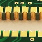
High speed circuit board Rogers PCB aplication
China PCB Manufacturing, Shenzhen PCB Manufacturer, Making Circuit boards
PCB Contract manufacturer, PCB Fabrication, Turnkey assembly services
Buy Print circuit board, customer: /USA/UK/Canada/South Africa...
PCB Supplier Shenzhen, China, PCB Manufacturer, Turnkey services
-
PCBSINO is the Top 5 PCB manufacturer company in China.
PCBSINO do rapid Prototype within 24 hours. our rigid PCB like MCPCB and Rogers PCB, FR4, High TG FR4, Rogers 4003, 4350,Al Aluminum metal Core MCPCB, Al2O3 Ceramic,Taconic,Halogen Free material, CEM-3, Fr2, CEM-1, CEM-2, 94VO, Rogers HF material, Polymide, etc.
PCBSINO making many type electronic product for our customer, Our turkey services team can source original components part for your project(Digikey/Mouser/RS...), senior Electronic engineer will follow each step of the production to solve any PCB problem and our team will do final function test in PCB house.
Express PCB |
|
Rigid PCB Rapid Prototype,24 hours |
| Fr4 PCB |
|
prototype Lower to 15USD ! |
| Rapid Prototype |
|
Fr4 Rigid PCB Rapid Prototype China, |
MCPCB |
|
MCPCB Manufacturer China, Shenzhen |
| Aluminum PCB: |
|
Aluminum Metal Core PCB manufacturing, Fabrication |
| Aluminum PCB: |
|
single side, double side MCPCB, 0.5-5mm or more |
Rogers 4350B |
|
Rogers 4350,Rogers 4003 Manufacturing |
| Rogers 4350B |
|
Rogers 4350B,4003C PCB Manufacturer |
| Ro4350B |
|
Rogers High Frequency PCB Manufaturing China |
Turnkey Services |
|
Turnkey PCB Assembly Services, |
| Turnkey services |
|
Print circuit board Manufacturing, Turnkey Services |
| Turnkey Assembly |
|
Through Hole PCB components wave soldering Assembly |
High speed circuit board Rogers PCB aplication
-
High speed circuit board Rogers PCB aplication
The PCB parameters that can be used for guidelines when choosing circuit materials for high-speed digital applications include Dk, dissipation, loss, and even dielectric thickness. The dielectric constant, Dk, of a PCB material has long been a guiding parameter for both analog and digital circuits since it is so closely related to the impedance of the circuits that will be fabricated on that material. Changes in a PCB material’s Dk, whether as a function of frequency, as a function of temperature, or for other reasons, can adversely affect the performance of broadband high-frequency analog circuits as well as high-speed digital circuits because it will change the impedances of transmission lines in unexpected ways. In particular, these unwanted changes in Dk and impedance result in distortion to the higher-order harmonics making up a high-speed digital signal, with loss of digital signal integrity. In general, PCB materials with low and stable Dk values with frequency and temperature will support high-speed digital circuits with low distortion of the higher-order harmonic signal components, as revealed by measurements with clean and clear eye diagrams for those high-speed digital circuits.
PCB materials are commercially available in many formulations at numerous performance levels, with the most usual tradeoff being between price and performance. A large number of parameters describe a circuit material’s performance, with dielectric constant (εr or Dk) probably the most popular starting point when comparing materials.
Economical RO4360 laminates provide performance similar to PTFE with the processing ease of FR-4. These glass-reinforced thermoset materials offer the same reliability that customers have come to expect from Rogers RO4350B™ laminates. They are fortified with ceramic filler to achieve mechanical stability as evidenced by a CTE of 30 ppm/°C in the z-axis and excellent thermal conductivity of 0.8 W/m-K.
Special materials are required to achieve the high frequency provided by this type of printed circuit board - any changes in the Er value of these materials can affect the impedance of the board. Many PCB designers turn to Rogers dielectric material for its lower dielectric loss, reduced signal loss, lower cost of circuit fabrication and better suitability for fast-turnaround prototyping applications.
Apart from choosing the appropriate PCB material and determining the correct the value of the Er, designers should take parameter such as conductor width and spacing, substrate constant into consideration. These parameters must be exactly specified and implemented with the highest level of process control.
RO4360 circuit materials are formulated with a dielectric constant of 6.15 in the z-axis at 2.5 and 10 GHz, enabling designers of antennas and power amplifiers to miniaturize their circuits while also reducing material costs. The low dissipation factor of 0.0038 at 10 GHz helps minimize signal losses, and the compatibility with standard automated assembly methods and the processing ease of FR-4 helps keep manufacturing costs low.
Rogers RT/duroid 6035HTC laminates are designed for applications where high reliability is required, including in circuits for military and aerospace systems. These high-performance materials incorporate a unique filler material to achieve a relative dielectric constant of 3.5 in the z-axis at 10 GHz with extremely high thermal conductivity of 1.44 W/m-K. RT/duroid 6035HTC circuit materials are ideally suited for high-frequency, high-power circuits, including amplifiers, couplers, filters, and power combiners/dividers. The high thermal conductivity, combined with a low loss tangent of 0.0013 at 10 GHz, enables circuit designers to optimize gain and efficiency in high-power amplifiers.
About Rogers Corporation
Rogers Corporation (NYSE:ROG) is a global technology leader in specialty materials and components that enable high performance and reliability of consumer electronics, power electronics, mass transit, clean technology, and telecommunications infrastructure. With more than 179 years of materials science and process engineering knowledge, Rogers provides product designers with solutions to their most demanding challenges. Rogers’ products include advanced circuit materials for wireless infrastructure, power amplifiers, radar systems, high speed digital; power electronics for high-voltage rail traction, hybrid-electric vehicles, wind and solar power conversion; and high performance foams for sealing and energy management in smart phones, aircraft and rail interiors, automobiles and apparel; and other advanced materials for diverse markets including defense and consumer products. Headquartered in Connecticut (USA), Rogers operates manufacturing facilities in the United States, Belgium, China, Germany, and South Korea, with joint ventures and sales offices worldwide. For more information, visit www.rogerscorp.com.
Special materials are required to achieve the high frequency provided by this type of printed circuit board - any changes in the DK/Er value of these materials can affect the impedance of the RF PCB circuit boards. Many PCB designers turn to special material for its lower dielectric loss, reduced signal loss, lower cost of circuit fabrication and better suitability for fast-turnaround prototyping applications. In addition to choosing the appropriate PCB material and determining the correct the value of the DK/Er, designers must take other parameter into consideration such as conductor width and spacing, substrate constant, etc. These parameters must be exactly specifiedand implemented with the highest level of process control. We're a High-Frequency PCB Manufacturer that takes the time to assess your needs
The Dk or relative permittivity of a circuit material is a measure of the capacitance or charge stored between two conductors on a dielectric material, compared to the same two conductors in a vacuum. Higher Dk values relate to higher flux densities, with the dimensions of microwave transmission lines (e.g., microstrip) diminishing with increasing values of Dk for a particular frequency.
Digital circuits continue to conquer higher speeds, with components such as microprocessors and signal converters routinely performing billions of operations per second. True, high-speed digital circuits can be flawed by such things as impedance discontinuities in transmission lines and poor plated-through-hole (PTH) interconnections between layers on multilayer circuit boards. But they can also be hurt by less-than-ideal choices of printed-circuit-board (PCB) materials for those high-speed-digital circuits. Which leads to the question: “What are the key parameters to consider when selecting a PCB material for a high-speed-digital circuit application?”
Analog circuit designers have learned to judge PCB materials by a number of important material parameters related to performance, such as dielectric constant (Dk) and dissipation factor (Df). These material parameters can also serve as yardsticks when comparing different circuit materials for high-speed digital circuit applications. In fact, it can be helpful to understand how high-speed digital signals are related to high-frequency analog signals when considering different PCB materials for those digital signals.
What is the highest frequency and fastest rise time in the system?
What are the electrical specifications at the inputs and outputs of the sinks and sources?
Are there sensitive signals to route – for example, think about controlled impedance, termination, propagation delay on a trace (clock distribution, buses, etc.)?
Is a microstrip adequate for the sensitive signals, or is it essential to use stripline technique?
How many different supply voltages exist? Does each supply voltage need its own power plane, or is it possible to split them?
Create a diagram with the functional groups of the system – e.g., transmitter path, receiver path, analog signals, digital signals, etc.
Are there any interconnections between at least two independent functional groups? Take special care of them. Think about the return current and crosstalk to other traces.
Clarify the minimum width, separation and height of a trace with the PCB manufacturer. What's the minimum distance between two layers?
What about the minimum drill and the requirements of vias?
Is it possible to use blind vias and buried vias?
As digital applications have continued to gain in speed, some of the general-purpose PCB materials typically selected for fabricating those circuits, such as FR-4, fall short in performance for various reasons. In many ways, the demands placed on a circuit material by high-speed digital circuits and their signals are similar to what is needed from those PCB materials by analog microwave and millimeter-wave signals.
Rogers offers three prepreg choices for bonding the 4350B laminates: a 4-mil prepreg that is available in two glass styles and one that is 3.6-mils thick with one glass style. Rogers discourages etchback of the material, advises against using a single layer of prepreg in high-layer-count, single-lamination stackups,and recommends cap construction. Manufacturers have to adjust the lamination cycle for fabricating boards when the Rogers material is involved because of the restriction on using a single layer of prepreg. The Rogers prepregs for the 4350B cores require higher pressure for proper lamination than do the Panasonic prepregs,which process no differently than conventional FR-4 materials.
Eight laminate thicknesses are available. Megtron 6 laminates come in 18 thicknesses, complemented by a wide range of prepreg thicknesses and glass styles, including various tightly woven, so-called flat-glass styles to avoid impedance variation caused by fiber-weave effect. Resin evenly coats the surface of those tight weaves. Three different percentages of resin content can be selected for several of the Megtron 6 prepreg glass styles. The most significant contrast betweem the Rogers material and the Panasonic material is that Megtron 6 laminates the same as conventional FR-4 materials; no incompatible pressures, temperature, movement, or cure time are involved.
What is the upshot of the differences between Rogers 4350B and Panasonic Megtron 6, beyond their raw material costs, considering that their electrical properties are alike? The most significant contrast is that Megtron 6 laminates the same as conventional FR-4 materials; no incompatible pressures, temperature, movement, or cure time are involved. Hybrid boards can be built in a single lamination with inner layers of relatively inexpensive FR-4 materials and an outer layer or layers of Megtron 6, using foil construction or cap construction. Moreover, the wider selection of Megtron 6 core and prepreg thicknesses and resin content eases stackup development and impedance control.
For example, a high-speed 10-Gb/s digital signal is a square-wave signal that can be viewed as a combination of different, but related, sine waves. A high-speed 10-Gb/s digital signal is comprised of different-frequency signal components, including a fundamental-frequency tone at 5 GHz, a third-harmonic signal at 15 GHz, a fifth-harmonic signal at 25 GHz, and a seventh-harmonic signal at 35 GHz (and, typically, harmonic signal components even higher than that).
Equipped with a professional and thriving high frequency PCB factory, Heros Electronics is an experienced high frequency PCB manufacturer who provides a reliable, superior-performing high frequency PCB fabrication service.
Specialized Materials of High-Frequency Circuit Board
Special materials are required to achieve the high frequency provided by this type of printed circuit board - any changes in the DK/Er value of these materials can affect the impedance of the RF PCB circuit boards. Many PCB designers turn to special material for its lower dielectric loss, reduced signal loss, lower cost of circuit fabrication and better suitability for fast-turnaround prototyping applications.
In addition to choosing the appropriate PCB material and determining the correct the value of the DK/Er, designers must take other parameter into consideration such as conductor width and spacing, substrate constant, etc. These parameters must be exactly specified and implemented with the highest level of process control. We're a High-Frequency PCB Manufacturer that takes the time to assess your needs
Heros Electronics’ Common-used High Frequency PCB Materials
We manufacture high-frequency PCBs with materials from Rogers, Arlon, Taconic, Isola and Teflon. The following table shows some of our common-used high frequency board materials.
Maintaining the signal integrity of a digital signal, and the sharpness of its rise and full times, is the equivalent of transferring millimeter-wave signals (the harmonics) with low loss and distortion. A PCB material capable of maintaining the signal integrity of high-speed digital signals at 10 Gb/s should also be capable of handling analog millimeter-wave signals through about 35 to 40 GHz with low loss and distortion. PCB material parameters that are critical to analog millimeter-wave circuit performance will also be important as guidelines for choosing PCB materials for high-speed digital circuits.
through-hole via in high-speed PCB will be investigated for increasing the transmission speed in PCB. First, the Rogers high-speed PCB is used and the vertical K-type connectors are used to connect measure equipment and PCB. The vertical K-type connectors are connected with signal traces by through-hole vias. The impedance mismatch
Getek
Loss tangent = .012 (slightly high) (usage in analog circuits up to 1.2 ghz and up to 2.0ghz in digital applications) (Stability in temperature variations good)Er = 3.5 to 4.3 (at 1.0mhz) (specific Er is dependent on glass-resin- ratio - Er is virtually constant form 1.0mhz to 2.0ghz)CTEr = +220ppm per degrees C (high). Tg is 180 degrees C.Electro-deposited Copper only. (helps in peel strength and de-lamination but somewhat limits etch width tolerance due to undercutting).
occurs at the through-hole via, so the design of the anti-pad is optimized. The anti-pad size is varied to compensate the impedance mismatch. The impedance of the through-hole via is increased from 44-Ω to 51-Ω. We have optimized the design of the anti-pad for the vertical K-type connectors connecting with signal traces. Next, the Rogers 3003 high-speed PCB is used, its transmission loss is lower and its transmission speed is higher than the Rogers 4350B PCB. The S-parameters of 5-cm signal traces in Rogers 3003 and 4350B PCBs are measured through a network analyzer. According to the S21 insertion loss, the 3-dB bandwidth is 21.3-GHz in Rogers 3003 PCB and the bandwidth is 9.58-GHz in Rogers 4350B PCB. The higher transmission speed in Rogers 3003 PCB can be verified. The design of the through-hole via between the upper-layer and lower-layer is also optimized. Using the Rogers PCB, the distance between the through-hole via and nearby ground vias and the size of anti-pad are varied to improve the impedance mismatch of signal path. The impedance of the through-hole via is increased from 47.6-Ω to 52.5-Ω, and the transmission bandwidth is improved and increased from 18.3-GHz to 24.5-GHz. The eye diagram of through-hole via transmission in Rogers PCB is also measured, and the clearer eye diagram can be obtained. We have optimized the characteristic impedances of the through-hole vias between the vertical K-type connector and signal trace, and between the upper-layer and lower-layer. The transmission bandwidths of the through-hole vias can be improved. The optimized deign can be applied in PCB of high-speed optical transceiver module.
Normally, layer count varies from four to eight layers for wearable devices. Layer structuring is such that if it’s an eight layer PCB, it provides enough ground and power plane to sandwich the routing layers. Thus, the ripple effect in crosstalk is kept to a minimum and electromagnetic interference or EMI is significantly reduced.
At board layout stage, the layout schedule is such that the ground plane is solid next to the power distribution layer. This creates a low ripple effect and system noise is reduced to virtually zero. This is especially important for RF subsystems.
FR4 has a high dissipation factor (Df) compared to Rogers’ material, especially at high frequencies. Df values for higher performance FR4 laminates are in the range of 0.002, an order of magnitude better than regular FR4. However, Rogers’ laminates are 0.001 or less. A meaningful difference in insertion loss is thus created when FR4 material is subjected to high frequencies. Insertion loss is defined as a loss of signal power in transmission from point A to B resulting from using a laminate such as FR4, Rogers, or other materials.
High technology circuit boards fabricated with high frequency laminates can be difficult to design because of the sensitivity of the signals and the challenges with managing the thermal heat transfer in your application. The best high-frequency PCB materials have low thermal conductivity versus the standard FR-4 material used in standard PCBs.
RF and microwave signals are very sensitive to noise and have much tighter impedance tolerances than traditional digital circuit boards. By utilizing ground plans and using a generous bend radius on impedance controlled traces can help make the design perform in the most efficient manner.
Greater concern regarding the glass weave effect is for high-speed and high-frequency circuits using a laminate with a single layer of woven-glass fabric. Using a microstrip circuit as an example, fabricated on a laminate with one glass weave layer, one concern has to do with the randomness of the glass weave effect when using woven-glass circuit materials and trying to achieve repeatable performance in high-volume production. Variations due to the glass weave effect can result in circuit-to-circuit performance variations. The random location of the woven-glass pattern as it relates to the circuit pattern can result in microstrip impedance variations that cause shifts in the phase angles of propagating high-frequency waves, resulting in degradation of any phase-sensitive signal characteristics, such as phase-based modulation.
While a laminate using multiple layers of a woven-glass fabric may help mitigate the glass-weave effect for high-speed and high-frequency circuits, multiple coupled or differential conductors on a single-layer circuit can expose additional problems with the glass weave effect. The degradation in conductor phase characteristics noted earlier can also impact coupled circuits or differential lines. Because such circuits have well-defined relationships between or among the conductors, each conductor requires the same wave propagation medium. If each conductor in a coupled pair has a different medium, they will not couple as expected. In pairs of differential lines, the phase angles will vary if the Dk values of the wave propagation medium varies between the pairs of lines. The end result is a slowing of the propagation of one signal wave versus the other, resulting in skew. Particularly in high-speed digital circuits, skew caused by the glass weave effect can significantly degrade performance due to changes in signal timing.
Changes in Dk due to the glass-weave effect can be moderated by fabricating a laminate with a filled resin system rather than an unfilled resin system. The filler typically has a different Dk value than the resin or the glass, and it fills the open spaces between the glass. The use of a filler results in a material with less-drastic changes in Dk in the small isolated areas between the glass bundles, with an effective averaging of the Dk values with the combinations of glass fabric, resin, and filler.
Another method is the use of spread/flat glass fabric along with minimizing the relative glass content in the laminate with respect to the filler and resin. This combination provides the mechanical benefits of glass reinforcement while minimizing the Dk variation along the signal propagation path.
Because wavelength of a circuit is frequency dependent and material dependent, PCB materials with higher dielectric constant (Dk) values can result in smaller PCBs as miniaturize circuit designs can be used for specific impedance and frequency ranges. Oftentimes high-Dk laminates (Dk of 6 or higher) are combined with lower cost FR-4 materials to create hybrid multilayer designs.
Understanding the coefficient of thermal expansion (CTE), dielectric constant, thermal coefficient, temperature coefficient of dielectric constant (TCDk), dissipation factor (Df) and even items like relative permittivity, and loss tangent of the PCB materials available will help the RF PCB designer create a robust design that will exceed the required expectations.
For a given frequency and characteristic impedance, conductors are wider for materials with lower Dk values, yielding less loss. The circuits on lower-Dk materials will have larger dimensions, but this may also mean higher yields for a particular circuit manufacturing process—all tradeoffs to consider when choosing a PCB material.
The dielectric constant of a vacuum, at 1.0, serves as the reference for other dielectric materials, such as Teflon with a dielectric constant of 2.1. Lower-Dk materials like Teflon or polytetrafluroethylene (PTFE) have often been used in RF/microwave circuits. However, the range of Dk values for high-frequency circuit materials is quite wide, from below 2.1 to above 10.0, for miniaturizing lower-frequency circuits with longer wavelengths.
Many suppliers can offer their manufacturing services, but few can match Power Design Services speed; Power Design Services’ turnaround times include FR4 (1-8 layers) and flex (1-4 layers) printed circuit boards in as little as a day, and even high-density multilayer PCBs (flex 20 layers) can be done within five days. Every project is treated with the utmost care, with a design review that optimizes PCB manufacturing and regular status teleconferences. Power Design Services has served Silicon Valley for more than 20 years, and its mission remains to be the preferred suppliers of PCB manufacturing services for companies around the world.
The dielectric constant of PCB materials will vary with humidity and temperature. Since water has a high Dk value of about 80, any material that absorbs water in a high-humidity environment will exhibit an increase in Dk, resulting in a change in high-frequency circuit performance. Changes in ambient temperature or from heat generated by high-power circuit components can also affect Dk, characterized by a parameter known as thermal coefficient of Dk (TCDk). For stable circuit performance, lower values are preferred, over the widest operating-temperature ranges possible.
Dedicated high speed laminates (like Rogers RO4350) have better properties at higher frequencies than FR 4 does. Using right materials would help designer to reach his design target easier and more reliably than with FR-4 material. The biggest trade off when a non FR-4 material is used is that the cost differential of the laminate is substantial.
Dielectric constant ( DK ε,Er)value need to be small and stable, high DK may cause signal transmission delay.
Dissipation factor (DF, tgδ) value need to be small, as it will affect quality of signal transmission, smaller DF could make sure smaller signal wastage.
The thermal expansivity need to be the same with copper foil as possible. If they are different may cause copper foil separated when the changes of cold and heat happen.
Heat resisting property, impact endurance, chemistry resisting, peel off resisting need to be good.
Water absorptivity need to be low, high water absorptivity will affect DK & DF when in the wet environment.
We support production of various high-frequency PCB from prototypes to production run in order to meet increasing demands of high-frequency PCB ,microwave PCB & RF PCB of our customers, include many of good performance high frequency PCB ,such as Rogers PCB, Ceramic PCB, Teflon PCB, Taconic PCB, Arlon PCB.
Firstly, a signal travelling through the printed circuit board has a velocity that is dependent on the dielectric constant of the printed circuit board. For example, when the signal frequency goes beyond 5 GHz, the typical dielectric constant of FR-4 (around 4.7) drops close to 4. However, the relative dielectric constant of the Rogers RO4350 material is constant (roughly 3.5) from 0 up to 15 GHz. If the dielectric constant of the printed circuit board changes versus frequency, then different frequency components of the signal will have different velocities. This means, that these components will reach the load at different times. As a result, this will be causing distortion of the digital signal.
Secondly, the signal losses due to printed circuit board material increase with frequency. Again, each harmonic of the digital signal will be attenuated according to that frequency of operation. Increased loss of the signal components will add to the distortion of the digital signal.
Then during our own manufacturing process, because we're also MIL-certified and AS9100 certified, we have process checks and process documentation to ensure that when we're manufacturing the board, it's seeing only processes that have been vetted and are monitored in performance, tracked, and managed. Once the finished product is done, we put it through construction integrity testing, full electrical testing, and then full dimensional and measurement testing before we ship it out to the customer.
Matties: Interestingly, I've looked at this in the supply chain from fabricator to assembler, and it seems to me that no matter how stable your processes are, you could be using best practices and all that but inspections are the only line of defense.
Hofer: Nothing is 100%. Even computers are 99.9999%, and that's not a hundred. Inspection is really the key to prevent escapes, because you're right, in manufacturing, in life, mistakes are going to happen and people are going to make mistakes and mistakes make people. It's how you move forward from them that's important. The inspection steps—which is why we have so many inspection steps along the way of manufacturing and at final—are the only way you keep it from getting out to assembly and then getting out into a product. Even that, unfortunately, is not at 100%. Sometimes things escape. We see it on the news all the time.
Matties: Absolutely. Airbags, ignition switches, falling satellites, or whatever it happens to be
Dispersion is a PCB material characteristic closely related to Dk. All PCB materials exhibit some amount of dispersion, which refers to the change in Dk as a function of frequency. A circuit material with minimal change of Dk with frequency will exhibit minimal dispersion, a good characteristic for high-speed digital circuits. Dispersion can be caused by a number of different circuit material traits, including the polarity of the dielectric material, the loss of the material, and even how the surface roughness of the copper conductor affects the PCB material loss at higher frequencies. If a PCB material exhibits different Dk values for the different harmonic signal components comprising a high-speed digital signal, it will cause losses and even shifts in frequency for those harmonics, resulting in degradation of the high-speed digital signals.
PCB signal losses at increasing frequencies, especially at the higher frequencies needed by a high-speed digital circuit’s higher-order harmonic signal components, can suffer excessive losses to the amplitudes of those higher harmonic signals, resulting in distortion to those high-speed digital signals. As noted in many earlier blogs, losses in a PCB can come from a number of different causes, including the dielectric material and the copper conductors.
The length of a high-speed digital circuit on a PCB material can also have a great deal to do with maintaining the integrity of those high-speed digital signals. Circuit losses for any PCB material are a function of frequency and will increase with increasing frequencies. A PCB material with acceptable losses within a bandwidth closer to the fundamental-frequency tone of a high-speed digital circuit, such as 5 GHz as in the earlier example, and perhaps even with low loss at the third-harmonic signal component, such as 15 GHz, may have excessive loss at the fifth- and seventh-harmonic signal components of that high-speed digital signal. In addition, signal losses are additive with length: a signal experiencing a loss of, for example, 0.5 dB per inch at 5 GHz for the first inch of a 10-inch-long high-speed digital circuit, will suffer loss of 5 dB at 5 GHz across the length of the circuit.
Rigid, Rigid-Flex and Flex
Roger, Arlon, Polyimide pcb’s
Laser microvias
Both blind and buried vias
Controlled depth drilling capabilities
High-density interconnect (HDI)
Extremely fine line circuitry
Ultra-fine pitch surface mount
RF/microwave applications
Utilizing high performance materials from Rogers, Taconic and Arlon
Commercial CAE tools, such as EM simulators, have traditionally relied on the “Morgan correlation,” as it is known, to account for the effects of conductor surface roughness when calculating the loss of high-frequency microstrip lines. Calculations usually involve a surface-roughness correction factor, Kr, which is a numerical factor based on a ratio of the smooth surface to the rough surface. In many cases, these calculations are quite good and will closely match measured results for conductor losses. But there are also many cases where the computer predictions and the measurements don’t match so closely. Such deviations can be costly at the design stage, possibly resulting in additional design iterations to achieve desired performance specifications. The deviations, and the delays, might be avoided by carefully considering the choice of a microwave PCB laminate in terms of its conductor surface roughness.
Most PCB substrates are clad with some form of copper conductor, including rolled-annealed (RA) copper, electrodeposited (ED) copper, or reverse-treated (RT) copper. As the name suggests, RA copper foils are formed by rolling an ingot of copper through a rolling mill. Successive passes through the mill can achieve a thin copper foil with good thickness consistency. ED copper is formed by depositing copper from a copper sulfate solution (bath) onto a slowing rotating, polished stainless-steel drum. The surface roughness of the copper on side of the stainless-steel drum is similar to that of the RA copper, although the copper surface is much rougher on the solution side of the deposition. RT foils are formed by producing low-profile foils on the bath side of the process, and plating the foil on the drum side.
Because the copper must adhere to different dielectric materials, such as FR-4 and polytetrafluoroethylene (PTFE) substrates, it is typically treated to increase adhesion. Of course, a perfectly smooth copper surface may not be the most ideal case for adhesion to a dielectric. Untreated copper film, formed by RA or ED process, has a surface that is covered by what might be thought of as small “teeth.” These jagged edges are ideal for forming a strong bond between the copper and the dielectric material. This same type of surface is less than ideal for use as a transmission line. But the foil-to-dielectric adhesion would be inadequate if using a perfectly smooth copper foil, one with a mirror-like finish. The solution lies in achieving a compromise in surface composition, to support the fabrication of low-loss conductors while maintaining good adhesion between the copper and the dielectric material.
Commercial PCB materials suppliers such as Rogers Corporation produce laminates with copper foils having numerous profiles as a result of the different levels of copper treatment. For example, PCB materials are available with standard copper conductor profiles which provide excellent adhesion of the copper to the dielectric material. Laminates are also offered with low-profile (LP) copper where the copper conductor surface is smoother to improve etch definition. This will also reduce conductor losses.
UMC Global manufactures Printed Circuit Boards, starting with simple Double Sided to Advanced Technology Multi Layer PCB’S. We offer High Temp & High Speed Materials, Controlled Impedance Designs, Chip On Board (COB) designs, Laser Drilled and Sequential Build Blind & Buried Micro Via’s, and fully RoHS compliant processes (Solder,Gold/Silver/Tin) and non-RoHS Tin/Lead solder.
LeitOn supports you with designing high frequency PCBs (HF-PCBs). We help you to find suitable substrates, to define the trace dimensions and to calculate the impedance effects for you. LeitOn has a wide range of HF-PCB base materials on stock and can deliver your high frequency PCBs within the shortest possible time. HF-PCB express service is also possible within 12 hours!
Your instructions for the designer should include: a brief description of the circuit’s functions; a sketch of the board that shows the input and output locations; the board stack up (i.e., how thick the board will be, how many layers, details of signal layers and planes—power, ground, analog, digital, and RF); which signals need to be on each layer; where the critical components need to be located; the exact location of bypassing components; which traces are critical; which lines need to be controlled-impedance lines; which lines need to have matched lengths; component sizes; which traces need to kept away from (or near) each other; which circuits need to be kept away from (or near) each other; which components need to be close to (or away from) each other; which components go on the top and the bottom of the board. You’ll never get a complaint for giving someone too much information—too little, yes; too much, no.
A learning experience: About 10 years ago I designed a multilayer surface-mounted board—with components on both sides of the board. The board was screwed into a gold-plated aluminum housing with many screws (because of a stringent vibration spec). Bias feed-through pins poked up through the board. The pins were wire-bonded to the PCB. It was a complicated assembly. Some of the components on the board were to be SAT (set at test). But I hadn’t specified where these components should be. Can you guess where some of them were placed? Right! On the bottom of the board. The production engineers and technicians were not very happy when they had to tear the assembly apart, set the values, and then reassemble everything. I didn’t make that mistake again.
RF board standards:
1,In the design of miniwatt RF PCB, main material is standard FR4 (Good insulation characteristics
uniform material, dielectric constant ε = 4,10%).
2,In the RF PCB, every component should compact configuration to ensure that the shortest connection
between the every component.
3, For a mixed-signal PCB, RF and analog section should stay away from digital part
(This distance is usually more than 2cm, at least 1cm), the digital part of the ground should be
We offer advanced technology quick turn PCB’s from Prototypes to High Volume Production.
eSurface has a huge advantages in being able to produce circuits with tight tolerances. This is ideal for RF, Microwave, Hi-Speed and/or tight impedance controlled applications. Although IPC allows trace tolerances of +/- 20%, this range is entirely inadequate for most of these applications. This tolerance derives from the wide process window required for standard chemical etching. With eSurface, where we plate up the circuit, we have been able to control line definition down to ¼ mil tolerances. Since our entire circuit pattern definition is using a more stable and more controlled process, we can produce the more finely defined circuits.
Impedance Benefits: How tightly can you control impedances?
See above for Tolerance Benefits. In essence, by being able to control the traces better, we can also better control the impedance accuracy. Current industry standard is +/- 10% of the desired impedance value. With eSurface we can now dramatically improve this tolerance.
Bond Strength Benefits: Does eSurface produce a better bond between the copper and the bare laminate?
eSurface has a distinct advantage in being able to produce a better bond (or “peel strength”) improvement over standard chemical etching. In test cases, the actual laminate was torn off, before the bond from the copper to the laminate. For fine line circuits, the copper is also much more resistant to scratches and abrasions because of this bond improvement. This improvement has also demonstrated clear benefits for hi-temp applications and ruggedization
Thermal Benefits: Does eSurface help with hi-temp or environmental extremes?
See above for Bond Strength Benefits. In essence, by being able to form a better molecular bond between the copper and the laminate, the survivability of the end circuit board is much improved, since in many applications it is that bond that breaks down prior to the actual laminate!
Environmentally Clean or “Green” Benefits: Is eSurface toxic or considered a hazardous chemical?
eSurface is completely water soluble and environmentally friendly. In addition, under the fully additive process option, eSurface will eliminate the needs for many acids and hazardous chemicals currently being used in the industry. Since eSurface is within the circuit pattern process, no part of the eSurface covaler remains on the boards. It is completely washed off in the process.
Although there is no guarantee, a good layout starts with a good schematic. Be thoughtful and generous when drawing a schematic, and think about signal flow through the circuit. A schematic that has a natural and steady flow from left to right will tend to have a good flow on the board as well. Put as much useful information on the schematic as possible. The designers, technicians, and engineers who will work on this job will be most appreciative, including us; at times we are asked by customers to help with a circuit because the designer is no longer there.
Rigid PCB’s (up to 30 layers)
Flex & Rigid Flex (1 to 12 layers)
Controlled Impedance and Capacitance
Blind and Buried Vias, Micro Via, Chip On Hole & Stack Via Technology
Heavy Copper (up to 6 oz.)
Variety of surface finishes:
Including:
OSP (ENTEK PLUS)
HASL
Electroless Nickel/Immersion Gold
Electroless Nickel/Electroless Gold
For furhter information, please feel free to contact us, www.pcbsino.com