High frequency combiner Rogers PCB aplication
China PCB Manufacturing, Shenzhen PCB Manufacturer, Making Circuit boards
PCB Contract manufacturer, PCB Fabrication, Turnkey assembly services
Buy Print circuit board, customer: /USA/UK/Canada/South Africa...
PCB Supplier Shenzhen, China, PCB Manufacturer, Turnkey services
-
PCBSINO is the Top 5 PCB manufacturer company in China.
PCBSINO do rapid Prototype within 24 hours. our rigid PCB like MCPCB and Rogers PCB, FR4, High TG FR4, Rogers 4003, 4350,Al Aluminum metal Core MCPCB, Al2O3 Ceramic,Taconic,Halogen Free material, CEM-3, Fr2, CEM-1, CEM-2, 94VO, Rogers HF material, Polymide, etc.
PCBSINO making many type electronic product for our customer, Our turkey services team can source original components part for your project(Digikey/Mouser/RS...), senior Electronic engineer will follow each step of the production to solve any PCB problem and our team will do final function test in PCB house.
Express PCB |
|
Rigid PCB Rapid Prototype,24 hours |
| Fr4 PCB |
|
prototype Lower to 15USD ! |
| Rapid Prototype |
|
Fr4 Rigid PCB Rapid Prototype China, |
MCPCB |
|
MCPCB Manufacturer China, Shenzhen |
| Aluminum PCB: |
|
Aluminum Metal Core PCB manufacturing, Fabrication |
| Aluminum PCB: |
|
single side, double side MCPCB, 0.5-5mm or more |
Rogers 4350B |
|
Rogers 4350,Rogers 4003 Manufacturing |
| Rogers 4350B |
|
Rogers 4350B,4003C PCB Manufacturer |
| Ro4350B |
|
Rogers High Frequency PCB Manufaturing China |
Turnkey Services |
|
Turnkey PCB Assembly Services, |
| Turnkey services |
|
Print circuit board Manufacturing, Turnkey Services |
| Turnkey Assembly |
|
Through Hole PCB components wave soldering Assembly |
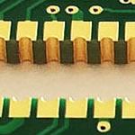
High frequency combiner Rogers PCB aplication
-
High frequency combiner Rogers PCB aplication
Key Specifications/Special Features:
PCB features:
Layer: 2
Material: Rogers 4003
Thickness: 0.5mm
Copper: 1oz
Mini hole: 0.2mm
Mini width/space: 0.2mm/0.2mm
Finish: immersion Tin
PCB specialties:
electronics high frequency circuit
PCB types: Rigid PCB/high frequency PCB/high TG PCB and more
PCB materials: FR4/Rogers/halogen-free/PTFE/PPO/PPE and more
PCB finish: HAL/LFHAL/ENIG/immersion tin/OSP
/immersion silver/flash gold/gold plated and more
PCB application: communication/medical/IoT/automobile/system control
/power & energy supply/consumer electronics/LED industry and more
Benefits for you
100% Tested quality, help you focus on core competencies.
Cutting-edge technology, handle well your special or complicated PCB
Save cost, increase your profitability
Save hassle, save your effort
Save time, upgrade your competitiveness
An excellent team, care what you care
Power dividers/combiners may be among the most popular and most used of high-frequency components. And couplers, such as directional couplers, are not far behind. These components help to divide, combine, and direct high-frequency energy from antennas and within systems with minimal loss and leakage, and the choice of printed-circuit-board (PCB) materials for these components can be a strong factor in approaching the ideal performance levels expected from each component. When designing and fabricating power dividers/combiners and couplers, it can be helpful to better understand how different PCB material properties relate to the final performance possible with these components, to help set limits on a number of different performance parameters, such as frequency coverage, operating bandwidth, and power-handling capability.
High-power PCBs inevitably generate heat, due to nonideal energy flow through a PCB’s copper conductors and its dielectric materials. The power, and resulting heat, may come from signals fed to a PCB from an external source to the input of the circuit or from a heat source, such as a power amplifier, on the PCB itself. Typically the goal is to flow the energy from the source on the PCB or from the input to the output of the circuit with as little heat generated as possible. Heat produced on a PCB results from a number of PCB material characteristics, including conductor losses, dielectric losses, dielectric constant (Dk), and dissipation factor (Df), and the high-power/thermal characteristics of different PCB materials can be quickly compared by means of their thermal conductivity (TC), a parameter that describes how effectively heat is transferred through a material as a function of applied or generated power. It is described in terms of watts of power per meter of material per degree Kelvin (W/m/K).
One of the first parameters to examine when comparing different PCB materials for high-power use is the TC, with higher values indicating efficient energy transfer and more effective capabilities to minimize heat rises in PCBs at higher power levels. A PCB material consists of circuit traces and ground planes formed of copper metal, with extremely high TC for good heat flow, and dielectric materials with much lower TC values. With a thermal conductivity of about 400 W/m/K, copper moves thermal energy very quickly from one location to another. Dielectric substrate materials have much lower TC values so that heat can build at interfaces between the copper and dielectric materials.
More than anything else, I'm hoping this is going to be educational, because I start off with some really basic ideas about insertion loss and why it is important, and then I get into how these different PCB fabrication influences can have an effect. One of the reasons I'm doing this is for people who may not know much about insertion loss, and that way they get a good introduction and overview of it. Then the other idea, I'm hoping, is that people who do know something about insertion loss and do circuit designs will now know more about some of these variables that they may not have known about before.
Because I've run into that from time to time, where an OEM or someone will come to us and say, "Hey, your material is not working right," and then we find out it's not really the material, it's something special or something funny that happened between the design and the fabrication. The more the designers know about these things the better, I think.
Matties: Communication is key. Could you give a quick overview of insertion loss for those of our readers that may not know anything about it?
Coonrod: Insertion loss, in an RF sense and in a frequency sense, is really the total loss of the circuit. The way to think about it is when you apply RF power on one end of the circuit, and you try to take power off the other end, you don't get the same amount of power you put into it because there's some loss there, and that's really what the circuit is doing. It's kind of a complicated issue where there are several other things that come into play, but it's really just how much loss the circuit really causes to an applied RF signal.
Matties: Is the variable the design, primarily?
ASC manufactures Single-sided, Double-sided and Multilayer circuit boards with metal cladding for improved thermal management and grounding. We manufacture high frequency PCBs with metal heatsinks for the telecommunication and aerospace industries. The heat sinks and PCBs are typically connected thermally and electrically. The metal heat sinks help with thermal dissipation and grounding of circuits.
ASC uses commercially available pre-bonded and post-bonded materials. Pre-bonded laminates are typically supplied by Rogers or Taconic. Post-bonding is done via commercially available sheet film adhesive materials, ASC’s patented sheet film adhesives or sweat solder. Some of the applications are RF Power Amplifiers, Splitters & Combiners, Complex Filters and RF Power Distribution. Some of the suppliers of laminate / dielectric materials we utilize are: Isola, Nelco, Rogers & Taconic. Metals include Aluminum, Copper, and Brass Composites.
TC values for circuit materials tend to be more indicative of materials that act as thermal insulators rather than as thermal conductors, which makes the task of removing heat from high-power circuits all the more challenging. The TC for low-cost FR-4 circuit materials, for example, is about 0.20 W/m/K. For lower rises in circuit temperature at higher power levels, a PCB material with higher TC value is required. RO4350B laminate has a considerably higher TC, at 0.62 W/m/K, while RO4360G2 laminate provides typical TC value of 0.80 W/m/K. Of course, for high-power RF/microwave applications where heat rises must be minimized, Rogers RT/duroid 6035HTC circuit material, with a TC value of 1.44 W/m/K, handles high power levels with minimal temperature rises. Rogers RT/duroid 6035HTC laminate is a fluoropolymer composite PCB material with a unique filler system for high thermal conductivity; it is available with reverse-treated, electrodeposited copper foil. This laminate features a low dissipation factor (loss tangent) of 0.0013 at 10 GHz, compared to dissipation factors of 0.0037 for RO4350B laminate and 0.0038 for RO4360G2 laminate.
A high-frequency PCB can meet your needs when incorporating a special signal requirement into your electronic components and products. It offers a frequency range of 500MHz - 2GHz, making it ideally suited for high-speed designs, as well as radio frequency (RF), microwave and mobile applications. These higher transmission frequencies can also provide the faster signal flow rates that are a necessity in today's increasingly complex electronic switches and other components.
A High-Frequency PCB Requires the Use of Specialized Materials
Special materials are required to achieve the high frequency provided by this type of printed circuit board - any changes in the Er value of these materials can affect the impedance of the board. Many PCB designers turn to Rogers dielectric material for its lower dielectric loss, reduced signal loss, lower cost of circuit fabrication and better suitability for fast-turnaround prototyping applications.
In addition to choosing the appropriate PCB material and determining the correct the value of the Er, designers must take other parameter into consideration such as conductor width and spacing, substrate constant, etc. These parameters must be exactly specified and implemented with the highest level of process control.
In addition to using materials that can handle power and heat with low loss, PCBs must be fabricated using conductive and thermal materials with closely matched coefficient of thermal expansion (CTE), so that any expansion or contraction of the materials due to power/temperature effects will occur at the same rate to minimize stress on the material interfaces, such as for plated through holes (PTHs) used to channel heat through a PCB.
But TC is just one parameter for comparing different PCB materials for high-power RF/microwave applications. While Dk is not one of the more critical material parameters when sorting through PCB material choices for high-power applications, circuit materials with lower Dk values yield circuits with wider conductor widths for a desired frequency and impedance. This results in less loss through those circuits (and less heat generated at higher power levels).
Another important material characteristic to consider for high-power applications is loss. A PCB with higher loss will generate more heat from the RF/microwave power it handles. The insertion loss from a circuit board consists of a number of different types of PCB-based losses, including conductor loss, dielectric loss, and radiation loss [which is typically dependent upon the type of transmission line, such as microstrip versus coplanar-waveguide (CPW) circuits]. Conductor losses can be affected by a number of different PCB characteristics, such as circuit material thickness, frequency, dielectric constant (Dk), conductor surface roughness, and even the finish on the PCB’s plated metal surfaces.
A wide range of circuits have been developed as power dividers (which serve as power combiners when used in reverse) and couplers, and they are available in many forms. Power dividers can be as simple as two-way dividers or as complex as N-way power dividers, with N a fairly large number as required by a system’s design. Many different directional and other coupler configurations have been developed over the years, including Wilkinson and resistive power dividers and Lange and quadrature hybrid couplers, in many different shapes and sizes. Matching a PCB material to any one of these circuit designs can help in the quest for achieving optimum performance.
These various circuit types offer tradeoffs in construction and performance, to help designers match them to different applications. A Wilkinson two-way power divider, which is designed to provide two output signals with equal amplitude and phase from a single input signal, is essentially a “lossless” circuit, designed to provide a pair of output signals that are each 3-dB less (or one-half the power level) than the input signal (with power dividers having more output ports suffering more loss per output port as a function of the number of outputs). In contrast, a resistive two-way power divider may provide a pair of output signals that are each 6 dB less than the power level of the input signal. The additional resistance in the signal path, while it adds loss, also adds isolation between the two signal paths.
High Frequency PCB or calls Microwave PCB / Radio Frequency PCB/RF PCB are widely used in wireless communications,wireless networks and satellite communications, in particular the popularity of 3G networks exacerbate the market demand for the product on the High Frequency PCB.Today, the demand for Microwave material PCB design is on the rise, Access to wireless high speed (high frequency) data is quickly becoming a necessity in multiple markets like Defense、Aerospace and Mobile Networks. Evolving market needs continue to drive forward development of High Frequency printed circuit board. like 50+ GHz microwave radios or defense airborne systems, also it can meet Halogen Free PCB together.
2. RF PCB & High-Frequency PCB made from polytetrafluoroethylene(PTFE PCB),ceramic filled fluoropolymer, or ceramic filled hydrocarbon thermosets materials with improved dielectric properties. this material have a low dielectric constant of 2.0-3.8, a low loss factor and excellent low loss characteristics, also with favourable properties are high glass transition temperature, a very low hydrophilic rate,an excellent thermal durability.The expansion coefficient of PTFE PCB material is similar to the copper which allows the material to exhibit excellent dimensional stability.
3.Panda PCB company has increased the investment of production equipment and research & development on High Frequency PCB field over the last few years,It is to meet to market development of the RF PCB for our customers from all around the world,We have rich experience in PTFE PCB manufacturing of various high-frequency circuit boards for quick turn prototypes and mass production.Our normal Teflon material supplier including: Rogers PCB, Nelco PCB,Taconic PCB, Arlon PCB...Detail please reference > About Us>PCB Materials.
The previous ROG blog offered guidance on selecting PCB materials for high-frequency circuits with coupled features, and much of that advice can be applied to any search for circuit materials for power dividers/combiners and couplers. As with many circuit designs, the dielectric constant (Dk) is often a starting point when surveying different PCB materials, and designers of power dividers/combiners and couplers generally tend towards using circuit materials with higher Dk values, since those materials support efficient coupling of electromagnetic (EM) energy using smaller circuit features than materials with lower Dk values. A problem with higher-Dk circuit materials, as the earlier blog explained, is the tendency towards anisotropic Dk characteristics across a circuit board, or having different Dk values in the x, y, and z axes of the circuit board material. Wide variations in Dk, also within one axis of the material, can make it difficult to achieve transmission lines with consistent impedance.
Quality practices
Strict PCB requirements complying and modification procedures.
High quality raw materials from Top suppliers for laminates,
copper foil, PP and more
Lean Manufacturing and continuous improvement.
100% E-test, inspections including AOI,
impedance control, soldering ability and more
Humane refund policy
Delivery & logistics
Samples in 1-5 days, volume order in 18days average
24 hours fastest quick turn service
Free samples/sample cost refund policy
Strong packing for long transportation
Best value-added service including shipping, warehousing and more
Advantage highlights
Specialized in two- to 32-layer PCB
ISO 9001-, ISO 14001-, ISO/TS 16949-, UL- and RoHS-certified
Partner of over 2000 small- and medium-scale customers
Two factory bases with over 15, 000 square meters
Less than 12 hours’ quick response
Widely acclaimed satisfying service beyond expectation
Above 66% PCB exported to international
PCB specialties:
PCB types: Rigid PCB/high frequency PCB/high TG PCB and more
PCB materials: FR4/Rogers/halogen-free/PTFE/PPO/PPE and more
PCB finish: HAL/LFHAL/ENIG/immersion tin/OSP
/immersion silver/flash gold/gold plated and more
PCB application: communication/medical/IoT/automobile/system control
/power & energy supply/consumer electronics/LED industry and more
Benefits for you
100% Tested quality, help you focus on core competencies.
Cutting-edge technology, handle well your special or complicated PCB
Save cost, increase your profitability
Save hassle, save your effort
Save time, upgrade your competitiveness
An excellent team, care what you care
Quality practices
Strict PCB requirements complying and modification procedures.
High quality raw materials from Top suppliers for laminates,
copper foil, PP and more
Lean Manufacturing and continuous improvement.
100% E-test, inspections including AOI,
impedance control, soldering ability and more
Humane refund policy
Delivery & logistics
Samples in 1-5 days, volume order in 18days average
24 hours fastest quick turn service
Free samples/sample cost refund policy
Strong packing for long transportation
Best value-added service including shipping, warehousing and more
Company culture
People matter most
Humility and discipline
Responsibility and accountability
Honesty and integrity
Maintain excellent work performance
Teamwork and love
Available substrates:
RO4350B RO4003C TLX-8 (TACONIC) F4B Woven Glass-Reinforced PTFE
4mil(0.1mm) 8mil (0.203mm) 20mil(0.5mm)
10mil(0.254mm) 12mil(0.3mm) 30mil(0.762mm)
13.3mil(0.338mm) 20mil(0.508mm) 40mil(1.0mm)
20mil (0.508mm) 32mil(0.813mm)
30mil(0.762mm) 60mil(1.524mm)
60mil(1.524mm)
For furhter information, please feel free to contact us, www.pcbsino.com