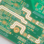
Impedance control of Multilayer PCB China, High-Speed Digital Circuit
Contract manufacturing of Impedance pcb, USB/HDMI differential Pair Impedance control
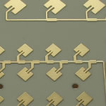
Differential Impedance 90 ohm,100 ohm, 110 ohm,120 ohm, 50 ohm single end Impedance
Impedance control |
|
Impedance control High Speed PCB |
| High-Speed |
|
Contract manufacturing of Impedance pcb, |
| Impedance control |
|
High-Speed Digital Circuit |
High-Speed |
|
High-Speed Digital Circuit |
| Impedance control |
|
Impedance control High Speed PCB |
| High-Speed |
|
Contract manufacturing of Impedance pcb, |
High-Speed |
|
differential Pair Impedance control |
| USB 90 ohm |
|
Differential 90 ohm,100 ohm, 110 ohm,120 ohm, |
| USB 90 ohm |
|
Impedance control of Multilayer PCB |
HDMI 100ohm |
|
Differential Impedance USB/HDMI/1394... |
| Impedance control |
|
Impedance control of Multilayer PCB |
| HDMI 100ohm |
|
differential Pair Impedance control |
RF 50 ohm |
|
50 ohm single end Impedance |
| Singl end |
|
Contract manufacturing of Impedance pcb, |
| RF 50 ohm |
|
Impedance control of Multilayer PCB |
Printed circuit boards with impedance requirements demand a high level of precision.
-
Printed circuit boards with impedance requirements demand a high level of precision.
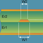
In the case of a microstrip, the impedance will depend on 4 parameters :
H, Er, T, W
For standard circuit boards, a PCB manufacturer is given a set of patterns - copper patterns, hole patterns, ink patterns, which are combined into a single circuit board with all the pattern sizes and positions within certain tolerances. Failure to meet a certain size or position with the specified tolerance can be cause for the circuit board to be rejected. If a trace has been defined as an impedance control trace, it is not the trace size which is strictly defined, but rather the impedance. While a nominal trace size will be provided in the Gerber layer, it is understood the circuit board manufacturer can vary trace width, height, and dielectric thickness as long as the final impedance is within tolerance.
What does impedance control on a PCB mean?
-
What does impedance control on a PCB mean?
I understand that when the electrical length is less than 1/10 of the trace length I would have to go in for impedance matching. A PCB impedance is controlled by its stack up. THat is thickness of prepreg, copper etc. So when a factory says it does impedance control , does it mean that they do that kind of a stack up? What does it mean when a factory says they will not do impedance control? Is it that they cannot do that stackup? If so , sticking to a normal 4 layer board stack is sufficient? What is th main FR4 specification that determines the impedance? Because right now I have a boards which has a stack up for 4 layers with thickness of each layer. DO I have to send this stack up to every PCB house and ask if they do this? How do I build these boards?
You have this backwards, the common rule is to use impedance control when the electrical length of the trace is more than 1/10 of a wavelength at the frequency of interest. (Like Rolf points out in his answer, the "frequency of interest" is more related to the rise and fall times of a digital signal than to the data rate)
It means they can control the thickness of the dielectric layer and the width of the trace with close enough tolerance to guarantee impedance matching to within some specified limits (often +/- 10%)
Also, like the other answer points out, they should have test equipment to allow them to verify the boards they produce.
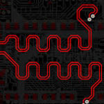
Impedance Control in PCB Design of High-Speed Digital Circuit
Impedance control technologies are quite important in high-speed digital circuit design in which effective methods must be adopted to ensure the excellent performance of high-speed PCBs.
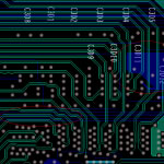
Impedance Calculation and Impedance Control of High-Speed Circuit Transmission Lines on PCB
• Equivalent Model on Transmission Lines
Figure 1 shows the equivalent effect of transmission lines on PCBs, which is a structure including tandem and multiple capacitor, resistor and inductor (RLGC model).
Impedance Control
THE BASICS
Electrical Impedance: A measure of opposition to time-varying electric current in an electric circuit
Simplified: To slow down an electrical circuit
Why: As flex circuit design and components become more complicated, smaller and faster, it becomes necessary to slow certain circuits down, allowing specific functions of components to perform before others. The increase in processor clock speed and component switching speed on modern flex circuit means that the interconnecting paths (traces) can no longer be regarded as simple conductors.
What is controlled impedance?
-
What is controlled impedance?
Probably the most common example of a controlled impedance component is the downlead (or feeder) connecting a receiving aerial to a wireless or television set. Aerial feeder leads usually take the form of "flat twin" cable (commonly supplied with VHF broadcast receivers) or low-loss coaxial cable. In both cases the impedance of the feeder is controlled by the physical dimensions and material of the cable.
Levels of Impedance Control
Typically, printed circuit boards are available with three levels of impedance control service.
1) Impedance Control – Most often used in high-end designs with a tight tolerance or unusual configuration. There are a number of different types of controlled impedance. The most common is referred to as characteristic impedance. Other types include wave impedance, image impedance, and input impedance.
First, the board is manufactured and then tested via a Time Domain Reflectometry (TDR) test to determine if impedance specifications are met; changes can be made if needed. It will be necessary to work closely with your circuit board supplier on impedance control specifications to achieve the best results. PCB Solutions has the expertise to ensure conformation to your impedance specifications.
2) Impedance Watching – This refers to compatibility in impedance. The impedance control trace will be indicated on the design. Width of the trace and height of the dielectric can be adjusted as needed. If necessary, a TDR test can be performed to check that impedance is correct. However, this does add some additional cost.
For furhter information, please feel free to contact us, www.pcbsino.com
 English
 Español
 Português
 Deutsch
 Français
 Italiano
 Россия
 Türkçe
 Polski
 Suid-Afrika
 بالعربية
 فارسی
فارسی