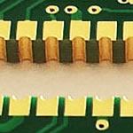
High Temperature Al2O3 Ceramic PCB aplication
China PCB Manufacturing, Shenzhen PCB Manufacturer, Making Circuit boards
PCB Contract manufacturer, PCB Fabrication, Turnkey assembly services
Buy Print circuit board, customer: /USA/UK/Canada/South Africa...
High Temperature Al2O3 Ceramic PCB aplication
-
High Temperature Al2O3 Ceramic PCB aplication
Tensky International Co., Ltd. is a leading Ceramic PCB Manufacturer and Ceramic Substrate Manufacturer manufacturer specialized in Ceramic PCB Manufacturer, Ceramic Metallization Service, Ceramic DPC Manufacturer, Ceramic Substrate Manufacturer, Electronic Ceramic Supplier, Thin Film Ceramic Substrates, CNC Metal Parts Manufacturer, AL2O3 Ceramic Supplier, ZRO2 Ceramic Supplier, High Temperature Ceramic Coating, Industrial Ceramics Manufacturer, Anti ESD Coating, Anti Glue Coating, and Silicon Carbide Coating Services. Tensky International
(Technology) Co., Ltd. mainly supply all kinds of electronic products and precision ceramic products, ceramic and fine porcelain, TSK adhere to build an international brand for the business goals and ideals, and in 2009 put into ceramic circuit board (substrate) of the R & D and production and a high-tech enterprises. After years of rapid development, starting from the development of fine ceramics, cross-sell fine ceramics to the world, then in, successfully entered the high power and high heat ceramic circuit board (substrate), and now TSK in mainland China in Shenzhen, Dongguan, Guangzhou, Foshan, Japan, South Korea, Russia, the United States and Germany Jieyou cooperation LED packaging manufacturers and suppliers to the needs of ceramic substrate factory, the products are widely used in high power LED ceramic substrate, microwave wireless communications, HCPV solar animal cells, ceramic sensor substrates, semiconductor and military electronics.
In this paper, carbon fiber with high thermal conductivity was introduced into the alumina-based composites. To avoid oriented alignment of carbon fibers (Cf) and carbothermal reactions during the sintering process, the Al2O3/glass/Cf substrate was hot-pressed under a segmental-pressure procedure at 1123 K. Experimental results show that carbon fibers randomly distribute and form a bridging structure in the matrix. The three-dimensional network of Cf in Al2O3/glass/Cf substrate brings excellent heat conducting performance due to the heat conduction by electrons. The thermal conductivity of Al2O3/30%glass/30%Cf is as high as 28.98 W mK−1, which is 4.56 times larger than that of Al2O3/30%glass.
STA different dimension super quality al2o3 ceramic substrate pcb
US $0.5-10 / Piece
50 Pieces (Min. Order)
STA Refractory (Zhengzhou) Co., Ltd.
In the high power module applications, the power increasing and the size shrinking becomes one of the major topics for the power module design. Due to both the power increasing and the size decreasing, the power density of the device will be much increased. Therefore, not only the thermal conductivity and stability of the substrate material but the long-term material reliability of the substrate have to be seriously considered. For these reasons, the ceramic PCB becomes one of the best solutions. The ceramic substrates now used are normally based on Ag-printed or direct bonding copper (DBC) technology. In the case of the Ag-printed ceramic substrate, the pattern resolution and metallization thickness are limited by the Ag-printed process. Also the combination strength of the silver and ceramic substrate by glass (which is normally mixed in the silver paste) is normally not good enough. A thermal dissipation barrier will then be formed between silver and ceramic substrate due to the poor thermal conductivity of the glass material. For the DBC ceramic substrate, DBC substrates are manufactured at 1065oC by the diffusion between ceramic and Cu /CuO layer. A thicker Cu layer thickness of normally more than 300 um is required in the thermal compressing bonding process. The Cu pattern resolution will then be limited by the
Product Description
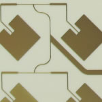
The Ceramic PCB products are combined the properties of heat dissipation of ceramic and conductive of metal , use the technology of precision automation printing or vacuum coating on the high precision ceramic substrate, make the ceramic substrate and the metal film sintered into integrated circuit with film as unit .
Alumina Ceramic Thin Plate are the main products of our company and sales all over the world are very good.
Mission ceramic provide high quality alumina ceramic products.
Our substrate are widely used for direct bond copper substrate (DBC), printer, LED and other high power circuit substrates and heat emission substrates of electronic components.
We can make any thickness as you need from 0.25 to 1.2mm. Max length we can provide is 280mm.
Supply alumina ceramic substrate:
Thickness: 0.3 - 2mm
Size: 10 - 300mm, According to drawing.
Laser Cutting ceramic substrate:
Cutting the highest accuracy: +/- 0.02mm
Cutting Maximum size: 152.4 x 152.4 mm
Cutting Minimum aperture diameter: 0.1mm
Cutting Maximum thickness: 1.5mm
Apart from MCPCB, if you want to use PCB in high pressure, high insulation, high frequency, high temperature, and high reliable and minor volume electronic products, then Ceramic PCB will be your best choice.
Why Ceramic PCB has such excellent performance? You can have a brief view on its basic structure and then you will understand.
96% or 98% Alumina (Al2O3), Aluminum Nitride (AIN), or Beryllium Oxide (BeO)
Conductors material: For thin, thick film technology, it’ll be silver palladium (AgPd), gold pllladium (AuPd); For DCB (Direct Copper Bonded) it’ll be copper only
Application temp: -55~850C
Thermal conductivity value: 24W~28W/m-K (Al2O3); 150W~240W/m-K for AIN , 220~250W/m-K for BeO;
Max compression strength: >7,000 N/cm2
Breakdown Voltage (KV/mm): 15/20/28 for 0.25mm/0.63mm/1.0mm respectively
Thermal expansion conefficient(ppm/K): 7.4 (under 50~200C)
According to different manufacturing method, current there’re three basic types for ceramic board:
A) Thick Film Ceramic Board
Thick Film Ceramic PCB: Using this technology, the thickness of conductor layer exceeds 10 micron, more thick than spurting technology. The conductor is silver or gold palladium, and was printed on ceramic substrate. More for Thick Film Ceramic PCB
Harsh environment capability
- Thermal shock test ( -40℃ ~ 125℃ )
- High Temp. and High Humidity ( 85℃ / 85% )
Good Thermal Conductivity ( white 20W/mk , Dark Violet 14W/mK )
Multi Layer Design
- LED Unit Inspection after Electrolytic Plating ( also Electro-less Plating )
- Ceramic Cavity type Design
- Ceramic Pocket Design for Zenor Diode on Flat type
Ceramic Materials Property
- Good for metallization and mechanically stable
- Color of Dark Violet & White
thickness of the Cu layer. However, the about 5~10% of the voids exist randomly between ceramic and Cu layer is the other major issue. The resolution issues of the Ag-printed and DBC ceramic substrates make the limitation for the device density design (fine line/width and flip-chip device design become very difficult). The glass material in the Ag printed ceramic substrate and the 5~10% voids existence in DBC ceramic substrate may cause the reliability issue operating at a high power density applications. For high power density module applications, we introduce the DPC technology on the ceramic substrate. In DPC ceramic substrate system, the sputtered Ti is used as the combination material between Cu and ceramic substrate. And the first copper is then sputtered on the top of Ti layer as seed-layer for the following Cu electrode plating (second cupper layer). By the material and the sputtering process control, several ceramic substrate raw materials can be used, such as Al2O3, AlN, BeO, Si3N4 and so on. The Ti combined/buffer layer provides good adhesion strength and material stability. The second copper layer is plated by electrode casting plating to 3 to 5 oz. (100~150um) in thickness. The key technology of the metal trace plating is the material control of the sputter layers and the second copper layer stress release during plating. In the DPC system, the double layers design is available. The laser drilled via holes on the
various ceramic substrates is introduced. The conducting of the front and back side is connected by the following plating process. The key technology of this process is the stability of the via-holes. We have to make sure the via-holes cleaning, impurity removing and material stability during high temperature laser drilled is well controlled. DPC ceramic substrates provide a better metal/ceramic interface uniformity and material reliability due to the stable Ti combination material and much less voids in the metal/ceramic interface. Also, the DPC ceramic substrates provide a gold pattern resolution of 50 um line space with tight tolerance of 20 um min. We believe the material characteristic make DPC a very suitable substrate material for high power module applications.
96% Al2O3 Ceramic Thin Plate/Ceramic Substrate
10000 Pieces (Min. Order)
Shenzhen Huaxin Precision Ceramics Co., Ltd.
e_Duration:Course Duration,Course_Level:Course Level,Standard_Type:Standard Type,Standard_SubType:Standard SubType,Standard_Topic:Standard Topic,Standard_Modifier:Standard Modifier,Ics_Terms_1:Ics Terms 1,Ics_Terms_2:Ics Terms 2,Ics_Terms_3:Ics Terms 3,Supplemental_Items:Supplemental Items'; var SEARCH_FIELD_REFERENCES = new Array(); var SEARCH_FIELD_DISPLAYS = new Array(); var searchFields = ALL_SEARCH_FIELDS.split(","); for (var j = 0; j < searchFields.length; j++) { parts = searchFields[j].split(":"); SEARCH_FIELD_REFERENCES[j] = parts[0]; SEARCH_FIELD_DISPLAYS[j] = parts[1]; } var TEMP_PAGE_TAGGING = 'ON'; var wt_domain = 'statse.webtrendslive.com'; var wt_dcsid = 'dcs7nlnxvuz5bdjhyiihzogfg_6x8o'; var TEMP_SAT_PAGE_TAGGING = 'ON'; if(TEMP_PAGE_TAGGING && TEMP_PAGE_TAGGING == 'ON') { var PAGE_TAGGING = true; } else { var PAGE_TAGGING = false; } if(SAT_PAGE_TAGGING && SAT_PAGE_TAGGING == 'ON') { var SAT_PAGE_TAGGING = true; } else { var SAT_PAGE_TAGGING = false; } var refSite='http://ieeexplore.ieee.org'; var refSiteName="IEEE Xplore"; var applicationName = 'Xplore'; var MC_OPERATION_DELAY_TIMEOUT='5000'; var MC_ADDING_DELAY_MSG='Please wait.The selected item(s) is being added to the cart.'; var MC_TIMEOUT='60000'; var MC_OPERATION_DELAY_MSG_FLAG='true'; //content types var CONTENT_TYPE_PARAM = 'contentType'; var CONTENT_TYPE_BOOKS = 'Books & eBooks'; var CONTENT_TYPE_COURSES = 'Courses'; var CONTENT_TYPE_STANDARDS = 'Standards'; var CONTENT_TYPE_CONFERENCES = 'Conference Publications'; var CONTENT_TYPE_JOURNALS = 'Journals & Magazines'; var CONTENT_TYPE_EARLY_ACCESS = 'Early Access Articles'; //User Preferences var citFormat = ""; var dlFormat = "";
Al2O3 grown by atomic layer deposition could be proposed as a nonactive layer for back end processes in view of the integration of scaled phase change memory devices. In this paper we report on thermal characterization from 50 to 600 °C of amorphous Al2O3 thin films grown on thermally oxidized silicon substrate at a temperature of 100 °C and capped with a 30 nm thick Pt layer. The effects of low temperature deposition and of a post-deposition rapid thermal annealing process (RTP) on the thermal properties of the films are investigated using a modulated photo-thermal radiometry technique coupled with post-annealing morphological characterizations. Degassing process occurring at high temperature greatly affects the film surface quality, though measurements of the films after RTP show that the thermal conductivity of amorphous Al2O3 increases as a function of temperature from 1.8 W K−1 m−1 at 50 °C to 3.3 W K−1 m−1 at 600 °C. At the same time, the value of the thermal boundary resistance at the Pt-Al2O3 interface decreases from 1.02 × 10⁻⁷ K m2 W−1 at 50°C to 4.8 × 10⁻⁸ K m2 W−1 at 600 °C.
Alumina ceramic substrate ALN substrate
US $0.2-10 / Piece
20 Pieces (Min. Order)
Liling Xing Tai Long Special Ceramic Co., Ltd.
Alumina Oxide is one of the most cost effective and widely used substrate materials in microelectronic applications.
The standard for thick film substrates is the 96% Alumina which is widely used in the manufacturing of hyrbrid microelectronic circuits. The availability, low cost and technical qualites of 96% Alumina make it a cost effective option for building hyrbid devices. The substrates offer excellent electrical insulating properties, mechanical strength, good thermal conductivity, chemical durability and dimensional stability.
The standard for ceramic PCB board is 99.6% Alumina which is often used for sputtered, evaporated and chemically vapor deposited metals for the circuit's generation. The high purity and smaller grain size of the 99.6% Alumina allow the material to be smoother with less surface defects and to obtain a surface roughness of less than 1u-in. 99.6% Alumina offers high mechanical strength, low thermal conductivity, excellent electrical insulation, good dielectric properties and good corrosion and wear resistence.
Aluminum oxide(Al2O3) is a compound of aluminum and oxygen. It is the most general type among various aluminum oxides and called alumina. The naturally generated ones form ruby or sapphire, precious jewels.
Generally when grown into single crystal at a high temperature over 2,300℃ it is called sapphire and when the powder of Al2O3 is sintered at 1,650℃ it is used a lot for fine ceramics with purity of 99.5% or more.
Al2O3-3535 SMD The thin film porcelain Ceramic Substrate
AlN is a very unique material in that it is a ceramic, nonconductor, but has high electrical conductivity like metal.
nterface cracking was observed to initiate at the short edge of the bonded copper and deviated into the ceramic layer when the crack grew beyond the critical length of 0.1-0.8 mm. The interface crack deviated into the ceramic layer at different thickness and grew parallel to the interface layer between the ceramic layer and copper layer. The crack propagation stopped after certain cycles. The copper layer with 10-20 μm thick alumina inside was not split away totally from the ceramic layer. The ELCF life prediction model could predict the life of Al2O3-DBC substrates well under high temperature cyclic loading. The material constants in the extremely low fatigue life prediction model were obtained using thermal fatigue tests results.
Research limitations/implications
The influence of copper layer thickness and ceramic layer thickness on thermal cracking characteristics of DBC substrate should be studied in the future. Failure models should also be further investigated.
Originality/value
The failure model of Al2O3-DBC substrates under high temperature cyclic loading was studied. A method for predicting the life of the substrate samples under high temperature cyclic loading was proposed.
It is mainly applied for special uses like an electrostatic chuck to hold wafer electrically in the semiconductor processes, a heater in CVD process for which even temperature is important, and a nozzle or a pipe to flow gas in CVD process, etc.
AlN, having strong covalent bond, is hard to sinter and in the high temperature oxidizing atmosphere over 1,000℃ it is easily oxidized to form alumina. Even at an ordinary temperature by reacting to moisture it is easily oxidized to form alumina, generating ammonia.
High Purity Alumina Ceramic Tube 99 Al2O3
Origin : China
Brand Name : UNIPRETEC
Material : Alumina Ceramic
produced the wear-resistant ceramic introduced in the formulation with very similar lattice Al2O3 and Cr2O3 TiO2, while adding ZnO whiskers from Toshiba introduced during the sintering process and the formation of Al2O3 solid solution, played fine of grain, promote and enhance the sintering fracture toughness. Since the raw material is expensive, there is no other domestic manufacturers are using this formula.
I wear a fracture toughness of ceramic products KIC≥4.8Mpa / m2.
4. Install the firm
I take the most reliable way to ensure that the operation does not fall off:
A. triple ceramic liner, ceramic, rubber, steel curing process is mature and reliable.
In the ceramic surface before vulcanization process, we use a surface treatment agent of US imports. Curing the products even artificially liner bent 360 °, the ceramic will not fall off from rubber, vulcanized rubber and steel firm bonding. Install with bolts to ensure easy maintenance and post-installation firm.
B. combo ceramic liner and steel solid paste
The bonding ceramic liner and steel, we use imported special metal and rubber adhesive. The product has a strong adhesion, heat resistance, acid, corrosion, anti-aging characteristics. As I ceramic paste special adhesive rubber liner, using hundreds of clients over the past decade, the reliability is very good, so far, no case of product loss problems.
Ceramic and metal cooling agent is mainly applied to ceramic and ceramic composite liner rubber roller encapsulated paste, the organic glue strong bonding, while in contact with the liner device area, the impact is very suitable for large, badly worn material handling wear system, such as power plant coal handling system, steel, mining, cement, ports and other industries.
Description :
... protection tubes and insulating rods produced by UNIPRETEC are made of alumina ceramic (Al2O3 > 99%). Alumina ceramic possesses a high melting ... safety and stability are required.The size of the high temperature ceramic tubes & rods can be customized according to customers' re...
Keyword : ALUMINA CERAMIC TUBE, AL2O3 CERAMIC TUBE, HIGH PURITY ALUMINA CERAMIC TUBE 99 AL2O3
Gold plus trader
UNIPRETEC CERAMIC TECHNOLOGY CO.,LTD
[Country : China]
The fast development of electronic industries and stringent requirement of recycling waste electronics have produced a large amount of metal-containing waste sludge. This study developed a waste-to-resource strategy to beneficially use such metal-containing sludge from the production and recycling processes of printed circuit board (PCBs). To observe the metal incorporation mechanisms and phase transformation processes, mixtures of copper industrial waste sludge and kaolinite-based materials (kaolinite and mullite) were fired between 650 and 1250 °C for 3 h. The different copper-hosting phases were identified by powder X-ray diffraction (XRD) in the sintered products, and CuAl2O4 was found to be the predominant hosting phase throughout the reactions, regardless of the strong reduction potential of copper expected at high temperatures. The experimental results indicated that CuAl2O4 was generated more easily and in larger quantities at low-temperature processing when using the kaolinite precursor. Maximum copper transformations reached 86% and 97% for kaolinite and mullite systems, respectively, when sintering at 1000 °C. To monitor the stabilization effect after thermal process, prolonged leaching tests were carried out using acetic acid with an initial pH value of 2.9 to leach the sintered products for 20 days. The results demonstrated the decrease of copper leachability with the formation of CuAl2O4, despite different sintering behavior in kaolinite and mullite systems. This study clearly indicates spinel formation as the most crucial metal stabilization mechanism when sintering copper sludge with aluminosilicate materials, and suggests a promising and reliable technique for reusing metal-containing sludge as ceramic materials.
High Purity Alumina Ceramic Tube 99 Al2O3
Origin : China
Brand Name : UNIPRETEC
Material : Alumina Ceramic
Diamond's (111) face can grow epitaxial GaN with wurtzite structure. Better still, single crystal AlN can be deposited directly on such diamond surface. Boron doped diamond has the highest mobility of holes, and silicon doped AlN can boost electron mobility. The AlN on diamond is capable to emit ultraviolet (UV) light with high intensity. Such UV light can excite phosphors for the emission of different colors, including white light with balanced RGB distribution. There are many possibilities of making super LED with diamond. Unfortunately, diamond wafers are not available commercially. However, synthetic diamond crystals can be made cheaply by a noval seeding technology (DiaCan{trade mark, serif}). These diamond crystals are embedded in a ceramic matrix to form diamond islands wafer (DIW). DIW is the enabling substrate for making super LED in the near future.
Description :
... protection tubes and insulating rods produced by UNIPRETEC are made of alumina ceramic (Al2O3 > 99%). Alumina ceramic possesses a high melting ... safety and stability are required.The size of the high temperature ceramic tubes & rods can be customized according to customers' re...
Keyword : high purity alumina ceramic tube 99 al2o3, alumina ceramic tube, al2o3 ceramic tube
Especially, in case where AlN green sheet is made by tape casting method which contains a lot of binder and the substrate or metalized substrate is made by multi-layer ceramic process, compared with the structural parts like PEC, ring, nozzle, tube, etc. made by general press molding method, the binder removing conditions which affects the control of the concentration of residual carbon, design of BN structure used for sintering and the sintering temperature condition for N2 atmosphere control are very important.
Physical properties: high insulation resistance, breakdown, high temperature resistance, abrasion resistance, high strength (three meters altitude fall not broken)
Fire rating: USA military standard MIL-F- (the highest level)
Typical application: strong current, voltage, strong high temperature parts, IC MOS, IGBT power tube heat pipe insulation
Certification: natural organic matter, the European Union, exempt products without certification materials
Thermal conductivity: high temperature: 1600 degrees below the ideal heat insulating material of high voltage and high frequency equipment
Application
Alumina ceramic is mainly used in large power equipment, IC MOS tube, IGBT chip heat conducting insulation, high frequency power supply, communication, mechanical equipment, strong current, high voltage, high temperature and other thermal heat insulation parts need products.
Physical properties: high thermal conductivity, high voltage insulation resistance, high temperature resistant, abrasion resistant, high strength
Product specifications:
Regular size and models :
The TO-220, 1mm*13mm*19mm
The TO-3 P, 1mm*20mm*25mm
The TO-264, 1mm*22mm*28mm
The T0-247, 0.635mm*17mm*22mm
Other non-standard products can provide drawings of custom processing
US $1-60 / Piece
1 Piece (Min. Order)
Shenzhen Kingsheng PCBA Tech. C
PCB Supplier Shenzhen, China, PCB Manufacturer, Turnkey services
-
PCBSINO is the Top 5 PCB manufacturer company in China.
PCBSINO do rapid Prototype within 24 hours. our rigid PCB like MCPCB and Rogers PCB, FR4, High TG FR4, Rogers 4003, 4350,Al Aluminum metal Core MCPCB, Al2O3 Ceramic,Taconic,Halogen Free material, CEM-3, Fr2, CEM-1, CEM-2, 94VO, Rogers HF material, Polymide, etc.
PCBSINO making many type electronic product for our customer, Our turkey services team can source original components part for your project(Digikey/Mouser/RS...), senior Electronic engineer will follow each step of the production to solve any PCB problem and our team will do final function test in PCB house.
Express PCB |
|
Rigid PCB Rapid Prototype,24 hours |
| Fr4 PCB |
|
prototype Lower to 15USD ! |
| Rapid Prototype |
|
Fr4 Rigid PCB Rapid Prototype China, |
MCPCB |
|
MCPCB Manufacturer China, Shenzhen |
| Aluminum PCB: |
|
Aluminum Metal Core PCB manufacturing, Fabrication |
| Aluminum PCB: |
|
single side, double side MCPCB, 0.5-5mm or more |
Rogers 4350B |
|
Rogers 4350,Rogers 4003 Manufacturing |
| Rogers 4350B |
|
Rogers 4350B,4003C PCB Manufacturer |
| Ro4350B |
|
Rogers High Frequency PCB Manufaturing China |
Turnkey Services |
|
Turnkey PCB Assembly Services, |
| Turnkey services |
|
Print circuit board Manufacturing, Turnkey Services |
| Turnkey Assembly |
|
Through Hole PCB components wave soldering Assembly |
For furhter information, please feel free to contact us, www.pcbsino.com