High-frequency coupler Rogers PCB aplication
China PCB Manufacturing, Shenzhen PCB Manufacturer, Making Circuit boards
PCB Contract manufacturer, PCB Fabrication, Turnkey assembly services
Buy Print circuit board, customer: /USA/UK/Canada/South Africa...
PCB Supplier Shenzhen, China, PCB Manufacturer, Turnkey services
-
PCBSINO is the Top 5 PCB manufacturer company in China.
PCBSINO do rapid Prototype within 24 hours. our rigid PCB like MCPCB and Rogers PCB, FR4, High TG FR4, Rogers 4003, 4350,Al Aluminum metal Core MCPCB, Al2O3 Ceramic,Taconic,Halogen Free material, CEM-3, Fr2, CEM-1, CEM-2, 94VO, Rogers HF material, Polymide, etc.
PCBSINO making many type electronic product for our customer, Our turkey services team can source original components part for your project(Digikey/Mouser/RS...), senior Electronic engineer will follow each step of the production to solve any PCB problem and our team will do final function test in PCB house.
Express PCB |
|
Rigid PCB Rapid Prototype,24 hours |
| Fr4 PCB |
|
prototype Lower to 15USD ! |
| Rapid Prototype |
|
Fr4 Rigid PCB Rapid Prototype China, |
MCPCB |
|
MCPCB Manufacturer China, Shenzhen |
| Aluminum PCB: |
|
Aluminum Metal Core PCB manufacturing, Fabrication |
| Aluminum PCB: |
|
single side, double side MCPCB, 0.5-5mm or more |
Rogers 4350B |
|
Rogers 4350,Rogers 4003 Manufacturing |
| Rogers 4350B |
|
Rogers 4350B,4003C PCB Manufacturer |
| Ro4350B |
|
Rogers High Frequency PCB Manufaturing China |
Turnkey Services |
|
Turnkey PCB Assembly Services, |
| Turnkey services |
|
Print circuit board Manufacturing, Turnkey Services |
| Turnkey Assembly |
|
Through Hole PCB components wave soldering Assembly |
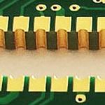
High-frequency coupler Rogers PCB aplication
-
High-frequency coupler Rogers PCB aplication
Microwave/RF PCB & High Frequency PCB uses materials of excellent dielectric property for its main body with other dielectric materials and metal substrates matched to complete corresponding multi-layer processing or thick-film processing and manufacture and to achieve the transmission functions of excellent high thermal conductivity, low dielectric constant, high frequency and high speed.
RF PCB are widely used in microwave transmission, Automobile telephone, wireless networks, wireless communications and satellite microwave communications, in particular the popularity of 3G networks exacerbate the market demand for the product on the RF PCB.
In order to meet increasing demands of Microwave & RF PCB for our customers all around the world, we have increased investment and intensity of research & development on Microwave high frequency PCB over the last few years. We're now experienced in professional production of various high-frequency circuit boards from quick turn prototypes to production run. For most of RF PCB materials (such as: Ceramic PCB, Teflon PCB, Rogers PCB, Taconic PCB, Arlon PCB), we have sufficient inventory to ensure fast delivery.
The above graph contrasts the measured loss per inch of standard "glass epoxy" FR-4 PCB material, versus a low-loss, high-frequency Rogers RO4350B material. It can be seen that at higher frequencies, such as for PCI Express Gen3, Intel QuickPath Interconnect, and other differential buses, the frequency response difference is significant.
Higher PCB insertion loss can, depending on the design, lead to a collapse of the channel margin. More attenuation will close the eye vertically. And as transitions become less sharp, there will be more horizontal closure of the eye, and the timing interval may collapse.
To address this, it is necessary to specify the maximum allowable insertion loss to the PCB supplier. PCB loss can be reduced by:
Any PCB design you’ve worked on in the past has probably had larger pads than was necessary. This was done for obvious reasons. It makes it easier to fit a soldering iron on the pad, inspections are quicker, and component placement precision becomes less of an issue.
But with high speed designs, your board real estate is going to be at a premium, and every inch of space you can save will count towards making it all fit. In light of this, we recommend maintaining a minimum oversize for all of your pads at 0-5% of the size of the component pins. This is compared with a traditional oversize of around 30% for standard electronic designs.
Why the drop in space? Not only will this help to improve mechanical strength, but it’s also going to reduce your parasitic capacitance, which comes in handy when dealing with high frequencies. And most important, the less space you give to your pads the more room you’ll have for differential pairs, vias, and those high pin-count parts like FPGAs or ICs.
#6 – Route Your Signals for Maximum Shielding Benefits
The high frequency signals on your board are going to be emitting a ton of electromagnetic radiation as they travel from source to sink. And the last thing you want to happen is to have two signals interfering with each other or a nearby component. To avoid conflicts on your board and maximize shielding benefits for your signals, consider these guidelines:
Be sure to keep long, parallel signals on your board at a minimum to avoid any signal coupling or crosstalk.
Maintain as much distance as possible between your signal traces, and even consider routing signals on a separate layer if they’re going to be particularly noisy.
When routing signals on different layers, be sure to route them orthogonally to each other. That is, on one signal layer your traces will be routed horizontally, and on the other vertically, 45 degrees, etc.
Each layer is being routed in a different direction orthogonally to avoid coupling. (Image source)
#7 – Provide an Efficient Path for Current Return
On high speed designs, each of your signals is going to seek a route from source to sink along the path of least impedance. For system clocks and other high speed I/O devices, ensuring this smooth path of travel might require the use of a via. Without these, you might find yourself with currents spreading around splits in your ground plane, and in turn leading to a loss of signal integrity.
Transition vias can quickly get your traces from source to sink on high speed layouts. (Image source)
If you do find yourself using vias to return your currents to their termination, then make sure you use tightly coupled, impedance matched differential vias to ensure your signals arrive on time. And when placing your return vias, place them as close as possible to your signal vias to minimize the length your signal has to travel.
#8 – Use the 3W Rule to Minimize Coupling Between Traces
Having your transmission lines couple can spell bad news for the integrity of your signal in transit. And while there’s always the general rule of keeping traces as far apart as possible to minimize this risk, it gets a bit fuzzy when it comes to the execution.
If you’ve ever wondered how far you need to keep your traces from each other to minimize coupling, then use the 3W rule. It states that the separation between traces must be three times the width of a single trace when measured from center to center. You can also increase this separation from three to 10 times to get even greater gains on reducing coupling and crosstalk.
The 3W rule will keep your traces far enough as possible to minimize coupling. (Image source)
#9 – Use the 20H Rule to Minimize Plane Coupling
In addition to the risk of coupling for individual traces, you also have to worry about the coupling between power and ground planes on your layout. If these two couple, you’ll get RF radiation spilling off the edges of your board, called fringing.
To prevent this from happening, you’ll want to make any power plane that is adjacent to a ground plane smaller than the ground plane. This will allow any fringing to be absorbed into the ground plane instead of radiating out externally. How much smaller though? Use the 20ᐧH rule, which says to make your power plan 20 times smaller than the dielectric thickness between your adjacent power and ground planes.
The 20ᐧH rule helps to reduce coupling between power and ground planes. (Image source)
#10 – Finishing Off With General Routing Guidelines
To finish off our top 10 tips is routing, which really deserves a blog post of its own, and probably a book to address things like RF, microwave or antenna design. This list isn’t exhaustive, so be sure to seek out the advice of a seasoned engineer for application-specific routing techniques. Here we go:
90-degree no-no. The first is always to avoid using 90-degree angle bends in your traces. Right angled traces can lead to signal reflections.
Differential pairs. You’ll only get the benefits of electromagnetic field cancellation when both the signals in your differential pair have the same length and gap. This will likely require some length match tuning in your PCB design software.
Transmission lines. Take the time to carefully design your transmission lines with the use of microstrip or stripline traces. Microstrip traces will only provide one reference plane separated by a dielectric. If you need more shielding capabilities, then a stripline will place a trace between multiple ground planes and a dielectric.
New Solutions with High Speed Design
When working on your first high speed PCB design project, there are new issues that you’re bound to discover. It’s no longer just about fitting the puzzle pieces together until everything fits as it should. Now you have to worry about exactly what those signals in your traces are doing, and how they’re affecting the parts around your board. All of this really boils down to a problem of EMI. And as you dive deeper into the world of high speed design you’ll begin arming yourself with strategies and knowledge to combat EMI with EMC, or electromagnetic compatibility. So consider these top 10 tips just enough to get you started on your first project, there’s still so much to learn!
Ready to begin your first high speed design project? Autodesk EAGLE has all the tools you need including differential pair routing, blind/buried vias, length tuning, and more. Subscribe to EAGLE to get started!
Share
Subscribe for Updates
Stay up to date with the latest news, knowledge and tutorials for Autodesk EAGLE and electronics design.
SEND ME UPDATES
POST A COMMENT
Log In to leave a comment
RELATED ARTICLES
Power In Your Pocket: How a Battery Works for the Electronics Beginner
We’ve all got power in our pockets, but do you know how it works? Come learn about the inner workings of a battery if you’re a beginner electronics designer!
Escape Frustration PCB Library Work: SamacSys Open Letter
Are we doomed to endless frustration in our PCB library management work? Read an open letter from the desk of a frustrated engineer.
Kirchhoff’s Law for Complex Circuits
It’s time to stand on the shoulders of Ohm’s Law. Come learn how to analyze the voltage and current in complex circuits that include both passive and series resistance!
Privacy/Cookies (Updated) | Legal Notices & Trademarks | Report Noncompliance | Site map | © 2016 Autodesk Inc. All rights reserved
Rogers Corporation has introduced RT/duroid 6035HTC, a new high-thermal-conductivity (HTC) laminate material engineered for low loss in high-power circuits. The fluoropolymer composite material is ideal for RF and microwave applications in military and high-reliability (hi-rel) applications required to handle high power levels, such as power amplifiers.
The microstrip line based circuits are widely used in RF and microwave frequency range. The microstrip lines have a lot of advantages with ease of mounting passive and active elements at the top of substrate as the main asset. Among many other devices directional couplers are also often realized in microstrip technology. Structures that use coupled lines have two modes of propagation called even and odd one. The velocity of the signal traveling through coupled microstrip lines is different for even and odd modes, which degrades performance of microstrip couplers. The high isolation and directivity is not achieved within the coupler's operation frequency range. Usually the maximum achieved directivity is limited to 20 dB only [1]. This is a disadvantage compared to stripline couplers with directivity over 40 dB. In the past the problem of limited directivity of microstrip couplers has been thoroughly studied and several methods to overcome the problem have been given. Some of them required additional layers of dielectric placed above the microstrip lines [2]. Other methods use additional compensating elements soldered to the lines [3-6]. Compensating capacitances have been especially popular [3-5]. Even exotic changes of the coupled lines shape can be a solution [7] improving microstrip coupler performance. In this paper we propose a new method for realizing a high directivity microstrip coupler in completely planar form. Our idea follows the waveguide coupler realization in which holes in common wall between two waveguides provide electromagnetic coupling between waves in the waveguides [8]. In the simplest realization two holes located at the quarter of wavelength are enough to create the coupler. The coupling is through holes only and between holes
Rogers RT/duroid 6035HTC laminates feature a relative dielectric constant of 3.5 at 10 GHz, making them suitable for a wide range of circuits, including amplifiers, couplers, filters, and power combiners/dividers employed in avionic and other military and hi-rel systems. The laminates incorporate a unique filler material to achieve superior heat-transfer characteristics compared to other high frequency circuit materials with similar dielectric constant.
RT/duroid 6035HTC laminates exhibit outstanding thermal conductivity of 1.44 W/mK as well as low loss, with a loss tangent of 0.0013 at 10 GHz, for excellent high frequency performance. This combination of high thermal conductivity and low dielectric loss translates into improved amplifier performance.
The high thermal conductivity and low loss of RT/duroid 6035HTC result in excellent heat transfer away from high-power devices, such as transistors, for improved circuit and device reliability. RT/duroid 6035HTC laminates are fabricated with thermally stable, reverse-treated and electrodeposited copper foils. These low-profile copper foils help minimize conductor losses in high frequency circuits, with the thermal stability needed for high reliability in high-temperature applications, even at the power levels found in many military electronic-warfare (EW) and commercial communications systems.
Development of distributed element filters began in the years before World War II. A major paper on the subject was published by Mason and Sykes in 1937.[8] Mason had filed a patent[9] much earlier, in 1927, and that patent may contain the first published design which moves away from a lumped element analysis.[10] Mason and Sykes' work was focused on the formats of coaxial cable and balanced pairs of wires – the planar technologies were not yet in use. Much development was carried out during the war years driven by the filtering needs of radar and electronic counter-measures. A good deal of this was at the MIT Radiation Laboratory,[11] but other laboratories in the US and the UK were also involved.[12][13]
Some important advances in network theory were needed before filters could be advanced beyond wartime designs. One of these was the commensurate line theory of Paul Richards.[14] Commensurate lines are networks in which all the elements are the same length (or in some cases multiples of the unit length), although they may differ in other dimensions to give different characteristic impedances. Richards' transformation allows a lumped element design to be taken "as is" and transformed directly into a distributed element design using a very simple transform equation.[15]
As an added benefit, RT/duroid 6035HTC laminates are formulated for ease of processing compared to other high-thermal-conductivity circuit materials employing alumina fillers. The special filler material in RT/duroid 6035HTC supports clean drill holes with minimal tool wear compared to alumina, for noticeably longer drill-bit lifetimes and higher drill-hole repeatability in volume production applications. The RT/duroid 6035HTC laminates are available in a variety of dielectric thicknesses and cladding options to support a wide range of high frequency circuit applicatio
About Cookies on this site:
Using wider traces
Providing for looser coupling (that is, greater spacing between traces)
Delivering thicker dielectrics (more laminate/prepreg layers and thicker layers)
Lowering the PCB material dielectric constant
The first two items tend to decrease routing density, which in turn usually requires more board layers, which can drive PCB cost up. And the third item also increases cost.
laminates are for designers seeking a cost effective high thermal conductivity PTFE material. These materials are designed for applications where high power RF signals demand improved PCB thermal management. With a combination of low loss tangent (0.0020 at 10GHz), high z-axis thermal conductivity (1.0W/m°K), low z-axis CTE (23 ppm/°C), and world class temperature phase stability (-9ppm/°C), TC Series laminates enable improved performance and reliability in high power applications. TC Series materials are ideal for high volume applications with panel sizes available as large as 48”x54”. TC Series materials are often chosen for applications such as power amplifiers and devices such as couplers, combiners, and dividers.
RO3003 laminates are ideal for loss-critical millimeter wave frequency designs, where consistent circuit performance matters, such as automotive radar sensors and point-to-point microwave backhaul communications systems. While already a benchmark for 77 GHz automotive radar sensors, RO3003 3.0 dielectric constant laminates are available with ½ ounce and 1 ounce rolled copper foil. Combining the very low dielectric loss of the RO3003 PTFE-ceramic resin system with smooth foil, results in high frequency circuit materials with best-in-class insertion loss. Also available with up to 0.040” thick copper plate.
XT/duroid laminates utilize PEEK (polyether ether ketone) based dielectric cores. PEEK is a high melting point polymer (Tm = 343C/649F) with excellent chemical and radiation resistance. This makes XT/duroid copper clad laminates an excellent choice for flex/rigid printed circuit boards that are exposed to harsh environmental conditions (e.g., aeronautics, oil & gas deep hole drilling, etc.) During the Large High Temperature Flexible Printed Circuits Board (LHTFPCB) project, under the European funded Clean Sky program, XT/duroid laminates passed more than 3700 hours at 260C (500F) continuously followed by 2x 8 hours vibration testing at 260°C (500F) without failure. XT/duroid laminates are available in various thicknesses starting at 2mil (50µm), are halogen free and inherently flame retardant. These laminates have very good dielectric strength, very low thermal resistance and provide excellent high frequency performance when utilizing low profile copper foil. Both the dielectric constant and dissipation factor are stable over a wide range of frequencies and temperature.
And the last item implies moving to more exotic materials, which also drives cost up.
There are numerous other factors that will affect insertion loss, including temperature, humidity, trace surface roughness (a major contributor), board topologies (i.e. routing lengths, number and type of connectors, via effects, backdrilling), any defects and variances within the board, etc. All of these need to be taken into consideration to ensure that system margins are acceptable. Further, the silicon itself eats into operating margins, and must be taken into consideration when providing insertion loss guidelines to the PCB supplier. In fact, it is known that the devices themselves contribute the majority of margin variance on any given design. An empirical study describing this last effect can be read in our white paper, Margins (Eye Diagrams) Follow the Silicon.
Mitigating these effects can be a challenge. It is always desired to keep costs down by continuing to use good old FR-4 and minimizing the number and thickness of layers. I'll write further on some design practices to help with this in a future blog.
RO4350B materials are proprietary woven glass reinforced hydrocarbon/ceramics with electrical performance close to PTFE/woven glass and the manufacturability of epoxy/ glass.
Providing tight control on dielectric constant and low loss while utilizing the same processing method as standard epoxy/glass, RO4350B is available at a fraction of the cost of conventional microwave laminates. No special through-hole treatments or handling procedures are required as with PTFE based microwave materials.
RO4350B materials are UL 94V-0 rated for active devices and high power RF designs.
Power Divider PCB
Power divider, is a way to the input signal energy is divided into two or more output equal or unequal energy devices, but also in turn multi-channel signal energy output all the way, this May also be referred to as a combiner. A power divider between the output ports should ensure a certain degree of isolation. Power divider according to the output is usually divided into one into two (one input two outputs), one three (one input three output) and so on. The main technical parameters of the power splitter are power loss (including insertion loss, distribution loss and reflection loss), the voltage standing wave ratio of each port, the isolation between the power distribution ports, amplitude balance, phase balance, power capacity and frequency band Width and so on.
Power divider PCB can use rogers ,Taconic,Arlon or Isola high frequency material,it is according to your design,the most important is DK and DF ,thickness
You can inform me DK,DF and thickness,we can recommend relative material for your reference
Coupler PCB
In the microwave system, always need to be a way of microwave power divided into a few proportion, which is the power distribution problem. Components to achieve this function known as the power distribution components that coupler, including: directional coupler, power distributor and a variety of microwave branch devices.
Coupler PCB just a part of coupler,but it is most important than all
So Coupler PCB require high technology and material
We have more than 7 years manufacture experience of coupler pcb,so you can send us your design file and requirements here , we will quote you within 1 hours, if scarce material, then will within 1 day
Plain old FR-4, with a higher loss and not tightly controlled Er[2]
Better specified Er[2] FR-4 derivatives (these may have better loss also)[3]
Specialized low-loss RF Materials with well specified Er values and much lower loss
It is a simple matter to go through the data sheets and make a spreadsheet that compares these items above one by one for comparison.
This can lead to a bewildering array of options, especially for the person new to RF. I have seen many cases where people new to RF have used expensive exotic materials for even low-frequency non-critical applications simply because someone said that the application was "RF" and they went into "Over-Specify Mode" just to be safe, but is this really needed?
Let's look at some real world applications:
High Volume / Cost Sensitive
Cell Phone
GPS Receiver
RF Remote Control
WLAN, Bluetooth, ZigBee et.al. Transceiver
Low Volume / High Performance
Test Equipment
Really high speed – bleeding-edge designs
In the high-volume cases you will be hard pressed to find anyone using really exotic materials in the under 6-GHz world. Take apart all the items that I just mentioned and you will find materials that look just like regular old FR-4. In the low-volume but high-performance category you will find board material that again looks like FR-4 and you will find higher-frequency materials, especially when the operating frequency exceeds 6 GHz.
In the low-volume cases, performance may be paramount and the circuit designs might be more complex. Many of these products do use a tighter specified type of "Glass Epoxy" or exotic RF materials. Mainly for their repeatability and for the trace losses.
How does FR-4 really perform?
General specification for Microwave/RF PCB
Layer count: 1-6
Board thickness: 0.2-3.2mm
Copper thickness: 0.5-4oz
Dielectric Constant(DK): 2.2-10.3
Min trace width/spacing: 4/4mil
Min drill hole size: 0.2mm
Surface treatment: HAL(Lead free), Immersion Gold/Tin/Silver, OSP, Gold Plating.
Material available: Teflon, Rogers, Taconic, Arlon, etc.
For furhter information, please feel free to contact us, www.pcbsino.com