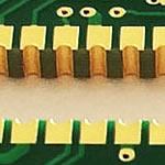
Motor driver Aluminum mcpcb aplication
China PCB Manufacturing, Shenzhen PCB Manufacturer, Making Circuit boards
PCB Contract manufacturer, PCB Fabrication, Turnkey assembly services
Buy Print circuit board, customer: /USA/UK/Canada/South Africa...
PCB Supplier Shenzhen, China, PCB Manufacturer, Turnkey services
-
PCBSINO is the Top 5 PCB manufacturer company in China.
PCBSINO do rapid Prototype within 24 hours. our rigid PCB like MCPCB and Rogers PCB, FR4, High TG FR4, Rogers 4003, 4350,Al Aluminum metal Core MCPCB, Al2O3 Ceramic,Taconic,Halogen Free material, CEM-3, Fr2, CEM-1, CEM-2, 94VO, Rogers HF material, Polymide, etc.
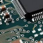
PCBSINO making many type electronic product for our customer, Our turkey services team can source original components part for your project(Digikey/Mouser/RS...), senior Electronic engineer will follow each step of the production to solve any PCB problem and our team will do final function test in PCB house.
Express PCB |
|
Rigid PCB Rapid Prototype,24 hours |
| Fr4 PCB |
|
prototype Lower to 15USD ! |
| Rapid Prototype |
|
Fr4 Rigid PCB Rapid Prototype China, |
MCPCB |
|
MCPCB Manufacturer China, Shenzhen |
| Aluminum PCB: |
|
Aluminum Metal Core PCB manufacturing, Fabrication |
| Aluminum PCB: |
|
single side, double side MCPCB, 0.5-5mm or more |
Rogers 4350B |
|
Rogers 4350,Rogers 4003 Manufacturing |
| Rogers 4350B |
|
Rogers 4350B,4003C PCB Manufacturer |
| Ro4350B |
|
Rogers High Frequency PCB Manufaturing China |
Turnkey Services |
|
Turnkey PCB Assembly Services, |
| Turnkey services |
|
Print circuit board Manufacturing, Turnkey Services |
| Turnkey Assembly |
|
Through Hole PCB components wave soldering Assembly |
Motor driver Aluminum mcpcb aplication
-
Motor driver Aluminum mcpcb aplication
RayMing is a quick turn Blank UL94V0 PCB Board Manufacturer
specialized in PCB prototype to mass production. The independent oversea marting department was found at the very begaining of our establishment to satisfy different PCB customers' demand. We are organized to provide our global customers with quality PCBs at a low cost.
Every blank pcb board is manufactured in compliance to standards adopted by ISO 9001 and IPC ,which ensures that the pcb is quality and the product manufacture is done as per the customer's environmental and regulatory requirements. We have thrived in a highly competitive printed circuit board industry primarily due to our unwavering commitment to meet the customer's specifications, quality and on-time delivery.
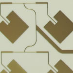
A simple layer single sided MCPCB consists of a metal base (usually aluminum, or copper alloy), Dielectric (non-conducting) Layer, Copper Circuit Layer, IC components and solder mask.
The prepreg dielectric provides excellent heat transfer from the foil and components to the base plate, while maintaining excellent electrical isolation. The base aluminum/copper plate gives the single-sided substrate mechanical integrity, and distributes and transfers the heat to a heat sink, mounting surface or directly to the ambient air.
The Single-Layer MCPCB can be used with surface mount and chip & wire components, and provides much lower thermal resistance than FR4 PWB. The metal core provides lower cost than ceramic substrates, and allows much larger areas than ceramic substrates.
Double Layers Metal Core PCB
Double layers MCPCB is consisting of two layers of copper conductor, put them on same side of metal core (usually aluminum, copper or iron alloy). The metal base is on the bottom of whole MCPCB, which is different from double sided MCPCB(the two copper layers were put on the each side of metal core respectively), and you can only populate SMD on top side.
Different with Single layer MCPCB, 2 layers MCPCB requires an additional pressing step to laminate the imaged thermal conductive laminate and metal core (also known as metal base) together.
Compared with normal FR4, this sturcture need more technology and experience on laminating of two layers together with metal core.
The processing steps of the MCPCB with the metal base embedded in the PCB are comparatively complex as hole plugging is required after primary drilling on the metal base in order to isolate it from the circuitry.
Double Sided Metal Core PCB
It also has same two layers of copper conductor like Double layers MCPCB, but the metal core is in the middle of two conductor, so there're conductors (trace) on both sides of metal core, and were connected to each other by Vias. So we named it "Double sided MCPCB", and you can populated SMD on both top and bottom.
Different with Single layer MCPCB, double sided MCPCB also requires an additional pressing step to laminate the imaged thermal conductive laminate and metal core (also known as metal base) together. But sometimes, some raw Metal Clad material vendor will supply board material which already laminated.
Compared with normal FR4, this sturcture need more technology and experience on laminating of two layers together with metal core.
Thermal Conductivities
Just for comparison, here are the thermal conductivities of various PCB materials. Note that these units are Watts per metre per Kelvin (or Watts per metre-Kelvin).
Copper:
Aluminum:
Water:
FR4:
Thermal prepreg:
Still Air:
Notice how traditional PCB prepreg has a very poor thermal conductivity at .
Design
Basic ones allow for components to be placed on one side only. White and black are common soldermask and silkscreen colours for IMS PCBs. More advanced ones follow normal stack-up rules, except one or more “cores” in the PCB is replaced with a metallic material. Prepreg and normal copper layers still used. However prepreg layers are small (typically 20-100um thick), and they have poor thermal conductivity! However we can’t make the dielectric too thin or the dielectric strength will be too low (and we will get breakdowns). Special prepreg can be used that is ceramic or boron-filled to increase it’s thermal conductivity while keeping it’s insulating properties.
An IMS PCB can be plated using most common plating techniques. However, HASL is not preferred due to the uneven surface it creates compared to other processes such as Cu-OSP, immersion Sn or NiAu (ENIG).
Single-Sided, Single-Layer IMS PCB
This is the most basic and cheapest IMS PCB design layout. It consists of one electrical layer sandwiched to a metallic substrate with some prepreg inbetween. It is commonly used for basic high-power LED PCBs and other simple circuits which don’t require too much routing.
General Information About Metal Core PCB
As Metal Core PCB means the base material for PCB is metal, but not normal FR4/CEM1-3, etc, and currently what the metal used are Aluminum, Copper alloy. MCPCBs are used instead of traditional FR4 or CEM3 PCBs because of the ability to efficiently dissipate heat away from the components. This is achieved by using a Thermally Conductive Dielectric Layer.
The main difference between a FR4 board and MCPCB is the thermally conductive dielectric material in the MCPCB.
where D is the via diameter and t is the plating thickness.
For a 0.6-mm diameter via with 35-μm (1 oz.) copper plating, the area (normal to the thermal pad) is only 0.06 mm2 compared to 0.28 mm2 for a solid via, resulting in a thermal resistance of 441 ºC/W per via compared to 96.8 ºC/W. For the same sized board and number of vias as in the previous example, the resulting through-plane thermal resistance becomes ~28 ºC/W.
However, the ability to create solid (copper) filled vias delivers additional reduced thermal resistance, as compared to vias filled with SnAgCu solder.
In general, increasing plating thickness during PCB production will improve thermal resistance of vias. Consult with your PCB manufacturer to determine if thicker plating is feasible.
Non-filled vias may become filled with solder during reflow. However, depending on a number of factors, this may not occur reliably. The vias, if not reliably filled, are not an effective heat management tool.
Other than creating a solid via during the plating process in PCB production, another option is to fill the vias with copper (or some other thermally conductive material such as conductive epoxy) as part of the PCB fabrication process. However, this adds an additional step to fabrication and may increase the cost of the board.
Solder voiding in open PTH vias
Figure 6a shows an example of unfilled vias after reflow, and Figure 6b shows an example of solder voids underneath the device (shown in red). The voids will increase the thermal resistance of the thermal interface. Also, the solder may overfill the hole leading to bumps on the bottom of the board which can reduce contact area between the board and heat sink. Steps can be taken to limit the amount of solder wicking. One way is to maintain a via diameter smaller than 0.3 mm. With smaller vias, the surface tension of the liquid solder inside the via is more capable of countering the force of gravity on the solder. If the via structure is constructed following the guidelines mentioned above, holding inside via diameter to 0.25 mm — 0.3 mm, minimal solder wicking is achieved. The drawback to this approach is that smaller open vias will result in a higher overall thermal resistance.
Figure 6a: Unfilled vias.
Bergquist aluminum based printed circuit board
Base Material: Bergquist material Aluminum pcb
Layers: 1
Thickness: 1.5mm
Copper thickness: 1Oz
plating process: Immersion gold
Description: LED MPCB
Bergquist HT-04503 Bergquist MP-06503 Bergquist HT-07006 Aluminium PCB, Aluminium printed circuit board, Aluminum PCB, Bergquist Aluminium base PCB, Bergquist Aluminium PCB, IMS PCB, LED PCB, Metal Core PCB, MCPCB, MPCB, High thermal conductivity aluminum pcb, aluminium based copper-clad pcb board, Bergquist T-clad Mcpcb, Bergquist Aluminum Clad Laminate PCB
Getting started with LED Aluminium PCB Prototyping
Afterwards ,when crucial decisions have been taken ..
( Type / numer of leds used ...Their arrangement ...Cooling calculations ...Light cone calculations ...etc ... )
First a pcb design has to be made ....
For that ,a pcb design software is needed ..(Personally, I use DipTrace )...
There ,according to led's maker suggestions/guide notes / solder pad dimensions , a " pad " has to be designed first ....
More or less ,is a "stamp " which is the led's solder power & thermal solder pads ...
In case of tiny ceramic leds ,dimensions are really small ...Set the "raster " at least at 0.05 mm
Follow makers suggestions/guide notes / solder pad dimensions,as close as possible ...
....
( In case of different leds used ,then for every type of led ,a "pad stamp " has to be made first .. )
Afterwards ,using the "pad stamp " ,a whole circuit can be designed ,with help of
Ruler tool , Thermal copper pouring ,manual or auto tracing ,etc ...
The easiest and fastest way to get 1 layer 10 to 1000pcs Aluminium PCBs prototype for an incredible low price while the production and quality control follows all industrial standards.
How it works:
Kindly choose the available options as shown above and send your PCB Gerber files that complies with all the limitations. You can upload the Gerber files after verifying the credentials. After this is done, simply just click “add to cart” and you’re good to go.
For bigger quantities, special options, tests, panels, discounts or combination with our other services, kindly contact us directly at pcb@smart-prototyping.com.
Combinations
If you want more than only a naked PCB, you can combine the PCB prototyping service together with our other electrical prototyping services into a turnkey solution:
3. COB MCPCB
COB MCPCB(known as Chip-on-Board Metal core pcb) is semi-conductor assembly technology, where micro-chip also known as die is electrically interconnected instead of using traditional assembly process or individual IC packaging on the final product board. COB MCPCB used in thermoelectric separation application products.
For normal MCPCB, there's a dielectric layer between trace copper and metal core, and the thermal conductivity is limited by that dielectric layers, so value can only be 1~3 W/m.K. But using COB MCPCB, there's no such dielectric layer because chip (die) direct touch the metal core, so thermal conductivity value of COB MCPCB will be almost the same one of metal core material itself. The normal material of metal core is aluminum, so thermal conductivity of COB MCPCB is more than 200W/m.K.
Material: Mirrow Aluminum
Number of Layers: 1 layers
Thickness: 1.6mm
Color of Solder Mask: White
Finished Immersion: Mirror Silver
4. Copper based PCB
Copper based printed circuit board
Base Material: Copper material
Layers: 1
Thickness: 3mm
Copper thickness: 1 Oz
plating process: Immersion gold
Description: Power LED MCPCB
Countersink holes+Countersink solt routing
Figure 6b: Solder voiding (not to scale).
-Fresh Etching solution (transparent ) might cause deposition of copper on exposed aluminium of pcb .
(at sidecuts...Back of pcb ,still has the protective plastic film on ..) ..
Afterwards ,when etching is done,those copper deposits ,go -off easily by water ...
But under them ,aluminium is ..etched ..Tiny black holes ,where copper was ..Not deep ..
But if pcb is cut exactly in final size and there's no "head room " for some file work ....
Then ...It's pretty bad ....
So better to use some used ( bluish ) etching solution ,in that case ..
Etching solution ,that already contains some diluted copper (bluish color ) ,does not
affect aluminium ..
Then ,that phenomenon ,completely disappears ...
A simple layer single sided MCPCB consists of a metal base (usually aluminum, or copper alloy), Dielectric (non-conducting) Layer, Copper Circuit Layer, IC components and solder mask.
The prepreg dielectric provides excellent heat transfer from the foil and components to the base plate, while maintaining excellent electrical isolation. The base aluminum/copper plate gives the single-sided substrate mechanical integrity, and distributes and transfers the heat to a heat sink, mounting surface or directly to the ambient air.
The Single-Layer MCPCB can be used with surface mount and chip & wire components, and provides much lower thermal resistance than FR4 PWB. The metal core provides lower cost than ceramic substrates, and allows much larger areas than ceramic substrates.
Double Layers Metal Core PCB
Double layers MCPCB is consisting of two layers of copper conductor, put them on same side of metal core (usually aluminum, copper or iron alloy). The metal base is on the bottom of whole MCPCB, which is different from double sided MCPCB(the two copper layers were put on the each side of metal core respectively), and you can only populate SMD on top side.
Different with Single layer MCPCB, 2 layers MCPCB requires an additional pressing step to laminate the imaged thermal conductive laminate and metal core (also known as metal base) together.
Compared with normal FR4, this sturcture need more technology and experience on laminating of two layers together with metal core.
The processing steps of the MCPCB with the metal base embedded in the PCB are comparatively complex as hole plugging is required after primary drilling on the metal base in order to isolate it from the circuitry.
3 ayer ersonalized etal ore Aluminium rinted ircuit oard apability layers 1 4layers ase material Aluminum opper ron Alloy hermal onductivity dielectrial layer m ithstand voltage
oard hickness 0 5mm 3 0mm opper thicknessup to 6 Z utline outing punching ut oldermask hite lack lue reen ed aiyo 4000 white egend ilkscreen olor lack hite urface finishing mmersion old A ax anel size 600 1200mm acking acuum lastic bag amples 4 6 ays ingle ayer etal ore A simple layer single sided consists of a metal base usually aluminum or copper alloy ielectric non conducting ayer opper ircuit ayer components and solder mask he prepreg dielectric provides excellent heat transfer from the foil and components to the base plate while maintaining excellent electrical isolation he base aluminum copper plate gives the single sided substrate
mechanical integrity and distributes and transfers the heat to a heat sink mounting surface or directly to the ambient air he ingle ayer can be used with surface mount and chip wire components and provides much lower thermal resistance than 4 he metal core provides lower cost than ceramic substrates and allows much larger areas than ceramic substrates ouble ayers etal ore ouble layers is consisting of two layers of copper conductor put them on same side of metal core usually aluminum copper or iron alloy he metal base is on the bottom of whole which is different from double sided the two copper layers were put on the each side of metal core respectively and you can only populate on top side ifferent with ingle layer 2 layers requires an additional pressing step to laminate the imaged thermal conductive laminate and metal
core also known as metal base together ompared with normal 4 this sturcture need more technology and experience on laminating of two layers together with metal core he processing steps of the with the metal base embedded in the are comparatively complex as hole plugging is required after primary drilling on the metal base in order to isolate it from the circuitry ouble ided etal ore t also has same two layers of copper conductor like ouble layers but the metal core is in the middle of two conductor so there re conductors trace on both sides of metal core and were connected to each other by ias o we named it ouble sided and you can populated on both top and bottom ifferent with ingle layer double sided also requires an additional pressing step to laminate the imaged thermal conductive laminate and metal core also known as metal base together ut sometimes some raw etal lad material vendor will supply board material which already laminated ompared with normal 4 this sturcture need more technology and experience on laminating of two layers together with metal core ulti ayers etal ore ust like 4 we can also make boards with more than 2 layers of traces and we named it ulti ayers he structure is similar with 4 ulti ayers but it much more complex to make ou can populated more components on the boards put signal and ground layer into seperated layers to achieve better performance in electrical performance ompared with normal 4 this sturcture need more technology and experience on laminating of more than two layers together with metal core and the cost is much higher than 2 layers or double sided Application of lights igh current potlight high current ndustrial power equipment igh power transistors transistor arrays push pull or totem pole output circuit to tem
pole solid state relay pulse motor driver the engine omputing amplifiers perational amplifier for serro motor pole changing device nverter ars firing implement power regulator exchange converters power controllers variable optical system ower voltage regulator series switching regulator converters A rinter driver large electronic display substrate thermal print head Audio input output amplifier balanced amplifier pre shield amplifier audio amplifier power amplifier thers emiconductor thermal insulation board arrays resistor arrays cs carrier chip heat sink solar cell substrates semiconductor refrigeration device Advantage 1 Aluminium factory directly 2 Aluminium ave the comprehensive quality control system 3 Aluminium good price 4 Aluminium quick turn elivery time from 48hours 5 Aluminium certificati
Double Sided Metal Core PCB
It also has same two layers of copper conductor like Double layers MCPCB, but the metal core is in the middle of two conductor, so there're conductors (trace) on both sides of metal core, and were connected to each other by Vias. So we named it "Double sided MCPCB", and you can populated SMD on both top and bottom.
Different with Single layer MCPCB, double sided MCPCB also requires an additional pressing step to laminate the imaged thermal conductive laminate and metal core (also known as metal base) together. But sometimes, some raw Metal Clad material vendor will supply board material which already laminated.
Compared with normal FR4, this sturcture need more technology and experience on laminating of two layers together with metal core.
-Etching solution lasts long ...You do not throw it away ,after it's first use ..
You just add water and etching agent -when needed -,in same first solution..
It can be used for many etchings ...
(kept in a plastic bottle ..I.e of water ... ) .
When colour has become really blue ,then you'll have to find a way ,to properly , "throw it away " / dispose it ...
It's a toxic for the environment chemical ...
It contains really high amounts of metallic copper!
Meaning it kills almost every aquatic organism..
...You do not flush it in the sink !
Another technique for limiting solder wicking involves using solder mask to restrict the flow of solder from the top side of the PCB to the bottom side. One process, called “tenting,” uses solder mask to prevent solder from either entering or exiting the thermal vias, depending on the side of the board to which the solder mask is placed. Tenting the bottom side with solder mask to cover and plug the thermal vias can prevent solder from flowing down into the via and onto the bottom of the board. In top side via tenting, small areas of solder mask are placed over the thermal vias on the top-side of the PCB to prevent solder from flowing into the vias from the top side of the board.
Figure 7: Tented vias with bottom-side solder mask (not to scale).
In general, Cree advocates creating copper-filled vias as being a more practical and effective technique, preferable to solder-filled vias.
3. Thermal performance simulations
The following section presents results obtained from computational thermal analysis for a series of PCB configurations 4.
3.1 Surface thermal dissipation
The first configuration, as shown in Figure 8, consists of a star FR-4 PCB with varying widths for the thermal pad and two board thicknesses (0.8 mm and 1.6 mm); the bottom copper layer is solid, and there are no thermal vias.
Advantage of MCPCB
1.heat dissipation
The purpose of a MCPCB is to efficiently remove the heat from all topical IC's (not just LEDs). The aluminum base and thermally conductive dielectric layer act as bridges between the IC's and heat sink. One single heat sink is mounted directly to the aluminum base eliminating the need for multiple heat sinks on top of the surface mounted components.
2. thermal expansion
Thermal expansion and contraction is the common nature of the substance, different CTE is different in thermal expansion. As its own characterics, aluminum and copper have unique advance than normal FR4, thermal conductivity can be 0.8~3.0 W/c.K.
Application of MCPCB
LED lights:High-current LED, Spotlight, high-current PCB
Industrial power equipment:High-power transistors, transistor arrays, push-pull or totem pole output circuit (to tem pole), solid-state relay, pulse motor driver, the engine Computing amplifiers (Operational amplifier for serro-motor), pole-changing device (Inverter)
Cars: firing implement, power regulator, exchange converters, power controllers, variable optical system
Power: voltage regulator series, switching regulator, DC-DC converters
OA: Printer driver, large electronic display substrate, thermal print head
Audio: input - output amplifier, balanced amplifier, pre-shield amplifier, audio amplifier, power amplifier
Others:Semiconductor thermal insulation board, IC arrays, resistor arrays, Ics carrier chip, heat sink, solar cell substrates, semiconductor refrigeration device
Beijing Ruikai Electronic Co., Ltd. is a leading Insulated Metal Substrate and MCPCB supplier (Aluminum based PCB, Copper based PCB, etc) in China. All Ruikai products manufactured under ISO 9001 and ISO 14001 standards. Also, our products are UL approved and RoHS compliant. We are acknowledged as a respected and reliable partner for customers in the following industries:
1. LED lighting
2. LED TV
3. Automotive Electronics
4. Electric Vehicle
5. Power Conversion
6. Motor Drivers
7. Concentrator Photovoltaic
8. Audio
9. Aviation and Military Industry
Why US?
1. High Quality Products: Rich research, development and production experience, advanced facilities, strict quality control during the whole process of production.
2. Excellent Service: Fleet response, professional technical support, one-stop source from raw materials to finished circuit, perfect after-sales service;
3. Competitive Price
Advantage:
1.Aluminium PCB & LED PCB factory directly
2. Aluminium PCB & LED PCB Have the comprehensive quality control system
3. Aluminium PCB & LED PCB good price
4. Aluminium PCB & LED PCB quick turn Delivery time from 48hours.
5. Aluminium PCB& LED PCBcertification(ISO/UL E354810/RoHS).
6.8 years experience in exporting service
7.Aluminium PCB& LED PCB is no MOQ.
8.PCB is high quality.Strict through theAOI(Automated Optical Inspection),QA/QC,fly porbe ,Etesting
Double layers MCPCB is consisting of two layers of copper conductor, put them on same side of metal core (usually aluminum, copper or iron alloy). The metal base is on the bottom of whole MCPCB, which is different from double sided MCPCB(the two copper layers were put on the each side of metal core respectively), and you can only populate SMD on top side.
Different with Single layer MCPCB, 2 layers MCPCB requires an additional pressing step to laminate the imaged thermal conductive laminate and metal core (also known as metal base) together.
Compared with normal FR4, this sturcture need more technology and experience on laminating of two layers together with metal core.
Beijing Ruikai Electronic Co., Ltd. is a leading Insulated Metal Substrate and Metal core PCB supplier (Aluminum based PCB, Copper based PCB, etc) in China. All Ruikai products manufactured under ISO 9001 and ISO 14001 standards. Also, our products are UL approved and RoHS compliant. We are acknowledged as a respected and reliable partner for customers in the following industries:
1. LED lighting
2. LED TV
3. Automotive Electronics
4. Electric Vehicle
5. Power Conversion
6. Motor Drivers
7. Concentrator Photovoltaic
8. Audio
9. Aviation and Military Industry
Why us?
1. High Quality Products: Rich research, development and production experience, advanced facilities, strict quality control during the whole process of production.
2. Excellent Service: Fleet response, professional technical support, one-stop source from raw materials to finished circuit, perfect after-sales service;
3. Competitive Price
The processing steps of the MCPCB with the metal base embedded in the PCB are comparatively complex as hole plugging is required after primary drilling on the metal base in order to isolate it from the circuitry.
Double Sided Metal Core PCB
It also has same two layers of copper conductor like Double layers MCPCB, but the metal core is in the middle of two conductor, so there're conductors (trace) on both sides of metal core, and were connected to each other by Vias. So we named it "Double sided MCPCB", and you can populated SMD on both top and bottom.
Different with Single layer MCPCB, double sided MCPCB also requires an additional pressing step to laminate the imaged thermal conductive laminate and metal core (also known as metal base) together. But sometimes, some raw Metal Clad material vendor will supply board material which already laminated.
Compared with normal FR4, this sturcture need more technology and experience on laminating of two layers together with metal core.
About RayMing Professional Aluminum custom pcb in China for led light
As a rich work experience in custom pcb,RayMing put the high quality as its priority criteria,in China Professional High quality Aluminum led light custom pcb has been very good reputation.Looking for Professional Low cost custom pcb in China for led light ,don't miss RayMing custom pcb.RayMing guarantee that give you high quality, the most ideal Professional Aluminum custom pcb for led light products .
Delivery Time Table (working day) for PCB Production as below,
1. <1m²:
For furhter information, please feel free to contact us, www.pcbsino.com