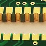
High frequency amplifier for communication Aluminum mcpcb aplication
China PCB Manufacturing, Shenzhen PCB Manufacturer, Making Circuit boards
PCB Contract manufacturer, PCB Fabrication, Turnkey assembly services
Buy Print circuit board, customer: /USA/UK/Canada/South Africa...
PCB Supplier Shenzhen, China, PCB Manufacturer, Turnkey services
-
PCBSINO is the Top 5 PCB manufacturer company in China.
PCBSINO do rapid Prototype within 24 hours. our rigid PCB like MCPCB and Rogers PCB, FR4, High TG FR4, Rogers 4003, 4350,Al Aluminum metal Core MCPCB, Al2O3 Ceramic,Taconic,Halogen Free material, CEM-3, Fr2, CEM-1, CEM-2, 94VO, Rogers HF material, Polymide, etc.
PCBSINO making many type electronic product for our customer, Our turkey services team can source original components part for your project(Digikey/Mouser/RS...), senior Electronic engineer will follow each step of the production to solve any PCB problem and our team will do final function test in PCB house.
Express PCB |
|
Rigid PCB Rapid Prototype,24 hours |
| Fr4 PCB |
|
prototype Lower to 15USD ! |
| Rapid Prototype |
|
Fr4 Rigid PCB Rapid Prototype China, |
MCPCB |
|
MCPCB Manufacturer China, Shenzhen |
| Aluminum PCB: |
|
Aluminum Metal Core PCB manufacturing, Fabrication |
| Aluminum PCB: |
|
single side, double side MCPCB, 0.5-5mm or more |
Rogers 4350B |
|
Rogers 4350,Rogers 4003 Manufacturing |
| Rogers 4350B |
|
Rogers 4350B,4003C PCB Manufacturer |
| Ro4350B |
|
Rogers High Frequency PCB Manufaturing China |
Turnkey Services |
|
Turnkey PCB Assembly Services, |
| Turnkey services |
|
Print circuit board Manufacturing, Turnkey Services |
| Turnkey Assembly |
|
Through Hole PCB components wave soldering Assembly |
High frequency amplifier for communication Aluminum mcpcb aplication
-
High frequency amplifier for communication Aluminum mcpcb aplication
Metal Core PCB MCPCB is kind of PCB with metal base material instead of woven glass (FR4), cotton paper (FR3) or others. It is with single layer metal core PCB, double layers MCPCB, double sided MCPCB, COB MCPCB and multilayer MCPCB. The common used metal core is aluminum, copper and alloy. Aluminum is the most frequently used among them due to its good heat transfer ability, dissipation ability and relatively cheaper cost than copper, although which may has a better performance.
Single Layer Metal Core PCB MCPCB consists of a metal base (aluminum or copper alloy), dielectric layer, and copper conductor layer. The single layer MCPCB can be used with surface mount and chip & wire components, and provides much lower thermal resistance than FR4 PCB. The metal core provides lower cost and allows much larger areas than ceramic substrates.
Metal Core PCB is used to replace traditional FR4 or CEM3 PCBs because of the ability to efficiently dissipate heat away from the components. This is achieved by using a thermally conductive dielectric layer.
the apparent diurnal revolution of the sun round the earth (Ps. 19:6), and the changes of the wind (Eccl. 1:6). In Job 22:14, "in the circuit of heaven" (R.V. marg., "on the vault of heaven") means the "arch of heaven," which seems to be bent over our heads.
Easton's 1897 Bible Dictionary electronics has the largest selection of in-stock electronic kits, robotic kits, test equipment & more. Our low prices, quick delivery, and easy & secure shopping experience keep our customers coming back for more. Serving hobbyists, schools, government, & corporations since 1996. We accept school & government purchase orders.
New Products and Gift Ideas! - Some of our latest Electronic Kits, Robot Kits, Test equipment, and Electronic Circuits! Lots of new items please check this page out!
10MHz Single Trace Oscilloscope - $179.95!
Sale! $11.95 OWI750 - Salt Water Fuel Cell Car Kit, Simply Amazing!
All Snap Circuits & Electronics Labs on Sale!
Parallax Boe Bot USB - $143.95
Elenco MX908 300 in 1 Electronics Learning Lab - Sale! $99.95
Back In Stock! Great Gift!
CK21533N - Football Robot Kit - Multi Player Capability! - $32.95
Sale! $39.95 OWI536 - OWI ATR 3 in 1 All Terrain Robot Kit
130 in 1 Electronics Lab
Learn to Solder Kit
Parallel Port Relay Board
Low Cost Digital Multimeter
Scrolling LED Sign Kit
The prepreg dielectric provides excellent heat transfer from the foil and components to the base plate, while maintaining excellent electrical isolation. The base aluminum/copper plate gives the single-sided substrate mechanical integrity, and distributes and transfers the heat to a heat sink, mounting surface or directly to the ambient air.
Security, Fire Alarm, Access Control and Camera industry, CCTV cameras and Mobile Security. Remote Accessible cameras, Intelligent Communication & Networking Solutions, electronic security equipment for homes, facilities, RVs, boats, perimeter fences, solar panels, locking and security door hardware. door hardware, key systems, CCTV, access control, and security solutions. Home Automation, Audio/Video, Security, and Surveillance,Lighting Controls, LED light, Searchlights, Progressive Meters, Progressive Systems, Bingo Hall Management Systems, Electronic Systems Equipment, Pull-tab Equipment, Satellite Systems, Gaming Equipment ,Drawing Equipment Manufacture, Instrumentation, Medical, Telecom, UPS, Automotive, Access Media and Infomobility, Aeronautic, Disk Drive Duplication Systems, Wireless Digital Data Radio Modem, Electronic Devices, Embedded Systems, Hard drive
The present invention relates generally to mm-wave receivers and transmitters in general and particularly to an integrated mm-wave device that employs a phased array.
2. Introduction
In recent years, the operating frequency of commercial communications and radar applications has also increased towards the upper end of the radio frequency spectrum, including operation at mm wavelengths. With the silicon chip assuming greater functionality at higher frequencies in a smaller area at a lower cost, it is becoming economically feasible to manufacture high-frequency wideband ICs for both commercial and consumer electronic applications. High- frequency wideband IC applications now include millimeter (mm) wave applications such as short range communications at 24 GHz and 60 GHz and automotive radar at 24 GHz and 77 GHz.
Technological developments permit digitization and compression of large amounts of voice, video, imaging, and data information. The need to transfer data between devices in wireless mobile radio communication requires reception of an accurate data stream at a high data rate. It would be advantageous to provide antennas that allow radios, especially wireless mobile devices, to handle the increased capacity while providing an improved quality that achieves antenna coverage in both azimuth and elevation. It would also be advantageous to provide mobile internet devices and/or access points with a smaller form factor that incorporates integrated, compact, high performance antennas.
DETAILED DESCRIPTION OF THE DISCLOSED EMBODIMENTS The subject matter regarded as the invention is particularly pointed out and distinctly claimed in the concluding portion of the specification. The invention, however, both as to organization and method of operation, together with objects, features, and advantages thereof, may best be understood by reference to the following detailed description when read with the accompanying drawings in which:
FIG. 1 is a block diagram illustrating devices using extremely high frequency radio signals to communicate in a wireless network in accordance to an embodiment
Thermal Conductivity:2.0W/m.k
Withstand voltage:DC≥6.0KV
Break-down voltage:AC≥6.0KV
Thermal Stress:300℃≥300S
Peel Strength:≥1.8N/mm
Features:
●Complied with ROHS &REACH .Halogen-free.
●Excellent thermal conductivity.
●Excellent insulation properties.
●Excellent reliability.
●No fiberglass contents.
●Good mechanical adaption.
●Electromagnetic dimensional stability.
●Good electromagnetic wave shielding.
Applications areas:
●High-Leung LED lighting /backlight module.
●High power electronic components(high power transistors,the entire flow device).
●Automotive(regulator,Power Supply Module)
●Audio(equalizer,amplifier)
Specification:
AL Substrate Layer :0.6mm;0.8mm;1.0mm;1.2mm;1.5mm;2.0mm;3.0mm.
Copper Foil: 1OZ; 2OZ; 3OZ; 4OZ.
Available Size:500*600mm; 600*1000mm; 500*1200mm
Customer tailor sizes are available.
When layout constraints required that a transmission line move to a different layer, it is recommended that at least two via holes be used for each transition to minimize the via inductance loading. A pair of vias will effectively cut the transition inductance by 50%, and the largest diameter via should be utilized that is compatible with the transmission line width. For example, on a 15-mil microstrip line, a via diameter (finished plated diameter) of 15 mils to 18 mils would be used. If space does not permit the use of larger vias, then three transition vias of smaller diameter should be used.
Signal Line Isolation
Care must be taken to prevent unintended coupling between signal lines. Some examples of potential coupling and preventative measures:
Base materials: high temperature FR4/FR5, free halogen FR4, aluminum based, polyimide, Rogers, argon and Teflon/PTFE
Layers: 1 to 30 layers standard PCB, blind and buried vias board
Finish: SMOBC/HASL, lead-free SMOBC/HASL, organic OSP, hard and soft gold, plating tin, immersion silver, immersion tin and electro less nickel/immersion gold
Surface copper thickness:
Maximum: 6/6oz
Minimum: 0.5/0.5oz
Hard gold thickness:
Maximum: 50U
Maximum board thickness: 6.0mm
Minimum track space: 4/4, 3mil partial allowed
Minimum size: 3 x 3mm
Maximum size: 1000 x 1200mm
PCB aluminum substrate is a metal circuit board material, by copper foil, thermal insulating layer and metal substrate composition, its structure is divided into three layers: line layer: equivalent to ordinary PCB CCL, line copper thickness Loz to 10oz. Insulating layer: Insulating layer is a layer of thermal insulating material with low heat resistance. Thickness: 0.003 "to 0.006" inch is the core of aluminum CCL operation, has been UL certified. Base: is a metal substrate, generally aluminum or can be selected copper. Aluminum based copper clad laminate and traditional epoxy glass cloth laminates.Aluminum Based PCB
PCB aluminum substrate features 1. PCB Aluminum Substrate Surface mount technology (SMT); 2. PCB aluminum substrate in the circuit design scheme has a good cooling performance; 3. PCB aluminum substrate can be reduced volume, reduce hardware and assembly costs; 4. PCB aluminum substrate can be replaced by ceramic substrates, to obtain better mechanical endurance; 5. PCB aluminum substrate can reduce temperature, improve product power density and reliability, prolong product life.Aluminum Based PCB
PCB aluminum substrate uses: office automation equipment: motor drives. Computer: CPU board ' bbs_ floppy drive ' power device, etc. Auto: Electronic regulator ' bbs_ igniter ' power controller, etc. Power module: Converter ' bbs_ solid relay ' rectifier bridge and so on. Communication Electronic equipment: high-frequency growth device ' bbs_ filter electric ' transmitter circuit. Power Equipment: Switch Regulator ' BBS_DC/AC Converter ' SW regulator, etc. Audio equipment: input, output amplifier, balance amplifier, audio amplifier, preamplifier, power amplifier and so on.
PCB aluminum substrate facing the challenge: PCB aluminum substrate facing the biggest challenge is more and more sophisticated and complex design, such as the increasing number of pins per chip, high-speed data flow technology and so on. However, the PCB aluminum substrate industry will continue to grow, the 2007 global PCB aluminum substrate output will exceed $50 billion trillion, is expected to reach the scale of $76 billion by The value of this product includes HDI, single panel, double panel, multilayer board, flexible plate, rigid-flex board, etc., including aluminum substrate, FR4, beryllium oxide and other substrates.Aluminum Based PCB
Click on the picture
or the link to play!
Circuit Game
Use a soldering iron to design a pathway for electricity to flow from the battery through the lightbulb and back again.
System Requirements
Kits
Amarino Evaluation Shield
23 October, Comments
After the success of BuildCircuit’s first Amarino Shield for Android-Arduino experiments, I am...
Amarino shield 3.0
4 September, Comments
MicroSD card breakout board – buildcircuit.com
2 September, Leave a comment
Simple experiment with Bluetooth and Arduino
1 September, Comments
4 in 1 DIY kit- dark sensor, latch circuit, astable multivibrator and clap switch
1 September, Comment
Simple ultrasonic range finder using HC-SR04
29 August, Comment
Amarino DZ863: Create Electrical Circuit Schematics Online
Ads by Google
Custom solutions from MNR Rubber Keypads, Membrane Switches PCB / FCB Assemblies, Touchscreens
www.MNRTechnology.com
Guia Texbrasil Where you find all about the Brazilian Fashion Industry.
www.abit.org.br/guiatexbrasil
Electronic Engineer Forum Collaborate, Debate, And Coroborate On The Connecting Edge
www.theconnectingedge.com
Lighted LED Switches Custom Pushbutton Switches, Buttons Indicator Lights, and Assemblies.
The Blobz Guide - Teach Simple Electronic Circuits To Children
The Blobz Guide - Teach Simple Electronic Circuits To Children
The Blobz guide takes the sort of simple electronic circuits that electrical engineering students first learn about, and presents them in a fun and entertaining way for a much younger audience.
Vertrieb von Kondensatoren Capacitor Sales
cir·cuit [sur-kit] Show IPA
noun
1.
an act or instance of going or moving around.
2.
a circular journey or one beginning and ending at the same place; a round.
3.
a roundabout journey or course.
4.
a periodical journey from place to place, to perform certain duties, as by judges to hold court, ministers to preach, or salespeople covering a route.
Newer semiconductor materials such as Gallium Nitride (GaN) and Silicon Carbide (SiC), with higher thermal conductivity and different CTE than Si and GaAs, require development of packaging materials that offer appropriate thermal properties, while also demonstrating improvements for manufacturability. The selection of materials made for a given device in an application is driven by reliability requirements and such factors as joining processes and joining materials, solder interconnections, fatigue failure potential under power and thermal cycling, maximum expected junction temperatures in transient and steady-state operating conditions; packaging density; package mounting and cooling; and cost. Reduction of CTE mismatch is critical to overall package reliability for many critical applications, especially with large and/or cyclical temperature gradients or significant overload conditions.
Development objectives
Development of GaAs and Gallium Nitride (GaN) semiconductor devices for RF and radar applications and Silicon Carbide (SiC) devices for high-temperature power devices is driving development of new substrate materials that have lower CTE values, similar to values for those semiconductor materials, and higher thermal conductivity (especially in the Z-axis). An important goal for cost and manufacturability is that new materials fit within existing PCB manufacturing processes. Reduced material weight is always important in aerospace and defense applications. A number of materials have been examined in one development program as candidates for development and production of organic PCBs with a high thermal conductivity, CTE-matched core.[1] Goals include manufacturability, process compatibility, and tested thermal performance capabilities of PCBs developed with new thermally-conductive core materials. One core material, a cast copper and graphite composite that has not previously been producible in large sheets (similar to what is required for PCB fabrication processes) was included in the development program. The manufacturer of the copper/graphite composite [2] subsequently developed manufacturing processes to allow production of 305mm x 457mm (12.0” x 18.0”) sheets of a thin version of this material. Following further process development, sheet thicknesses were reduced from the initial 1.02mm (0.040”) to the required 0.51mm (0.020”) to enable capture in-situ as a thermal core within organic multilayer PCBs for radar transceiver modules.
Use Arlon elements to the PCB fabrication of large efficiency and frequency dependent printed circuit manufacturing. With this particular, there is a growing demand for enterprises that will offer you manufacturing solutions for this kind of applications. Certainly one of the primary makes use of of an aluminum PCB board is within the LED lighting field, street lighting, etc. Some owners may look at trying to restore the damaged circuitry.
Now come across an edge in the paper and begin pulling it gently away from the copper. PCBs present a strong spot to put in the other components onto. Frequently, the style and design and manufacturing of the printed circuit board (PCB) is as significant since the layout of your primary circuit itself. In accordance to your China Securities Journal reported on September six, in actual fact, as early as June of this 12 months, the market came 3 Japanese organizations will integrate its modest LCD panel small business news.
A number of manufacturing devices may be intended with all the utilization of such companies. It can be a frequent truth that aluminum could be the most frequently used metal employed in electrical power transmission lines globally and it eliminates the impact of thermal strain on each of the modules. Therefore, the fabrication of this kind of PCB boards is carried out from the several manufacturing services companies which possess the certain machines for this process. Most respected producers will willingly give references on request.
When get hired you come with a bundle of perceived values which include educated, disciplined, trust worthy and would be an asset to your employer. A printed circuit board is usually rigid or versatile, based upon the material it can be made of and its end application. There are plenty of distinctive forms of hot tub circuit boards accessible. As an illustration, the main board on which the circuits are etched and established is called the motherboard.
Typically, through-hole and surface-mount construction has to be mixed in a single assembly because some required elements are available only in surface-mount packages, whilst others are available only in through-hole packages. Other regions include things like street lighting, buildings, landscapes and camping gear. These PCB boards are extremely trusted and long lasting and therefore supply very good output as compared to some others. In a amount of higher volume production runs, silk display printing is usually a popular approach.discover more here
RF Transmission Lines: Lines should be kept as far apart as possible, and should not be routed in close proximity for extended distances. Coupling between parallel microstrip lines will increase with decreasing separation and increasing parallel routing distance. Lines that cross on separate layers should have a ground plane keeping them apart. Signal lines that will carry high power levels should be kept away from all other lines whenever possible. The grounded coplanar waveguide provides for excellent isolation between lines. It is impractical to achieve isolation better than approximately -45dB between RF lines on small PCBs.
High-Speed Digital Signal Lines: These lines should be routed separately on a different layer than the RF signal lines, to prevent coupling. Digital noise (from clocks, PLLs, etc.) can couple onto RF signal lines, and these can be modulated onto RF carriers. Alternatively, in some cases digital noise can be up/down-converted.
VCC/Power Lines: These should be routed on a dedicated layer. Adequate decoupling/bypass capcitors should be provided at the main VCC distribution node, as well as at VCC branches. The choice of the bypass capacitances must be made based on the overall frequency response of the RF IC, and the expected frequency distribution nature of any digital noise from clocks and PLLs. These lines should also be separated from any RF lines that will transmit large amounts of RF power.
Ground Planes
The recommended practice is to use a solid (continuous) ground plane on Layer 2, assuming Layer 1 is used for the RF components and transmission lines. For striplines and offset striplines, ground planes above and below the center conductor are required. These planes must not be shared or assigned to signal or power nets, but must be uniquely allocated to ground. Partial ground planes on a layer, sometimes required by design constraints, must underlie all RF components and transmission lines. Ground planes must not be broken under transmission line routing.
Ground vias between layers should be added liberally throughout the RF portion of the PCB. This helps prevent accrual of parasitic ground inductance due to ground-current return paths. The vias also help to prevent cross-coupling from RF and other signal lines across the PCB.
Special Consideration on Bias and Ground Layers
The layers assigned to system bias (DC supply) and ground must be considered in terms of the return current for the components. The general guidance is to not have signals routed on layers between the bias layer and the ground layer.
Descriptions:
Based in China, Agile Circuit is specializes in printed circuits manufacturing with high quality and low cost by prototypes and low volume. Our products range includes FR4 rigid printed circuits, PCB aluminium, copper clad circuit boards and PCB assembly which are extensively used in communications, network, industrial control, computer applications, national defense, aerospace and medical fields.
Metal core PCB feature:
1. Use of surface mount technology (SMT)
2. Effective treatment of thermal diffusion in PCB circuit design
3. Reduce operating temperature, increase power density and reliability, extend the life of product
4. Smaller footprint, lower hardware and assembly costs
5. Replace the fragile ceramic substrates PCB with better mechanical durability.
Metal Core PCB Specifications
1 & 2 Layer Dielectrics
Up to 6 oz finished Cu
Aluminum, Copper and iron alloy base material up to .250" thick
HASL, ENIG ,OSP, Pb Free HASL finishing available
Metal Core Printed Circuit Board Custom PCB MCPCB for High Frequency Amplifier
Thermal Clad Metal Core PCB fabrication contact us for more details.
For furhter information, please feel free to contact us, www.pcbsino.com