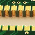
Aircraft array camera Aluminum mcpcb aplication
China PCB Manufacturing, Shenzhen PCB Manufacturer, Making Circuit boards
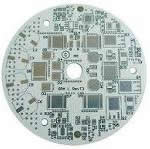
PCB Contract manufacturer, PCB Fabrication, Turnkey assembly services
Buy Print circuit board, customer: /USA/UK/Canada/South Africa...
PCB Supplier Shenzhen, China, PCB Manufacturer, Turnkey services
-
PCBSINO is the Top 5 PCB manufacturer company in China.
PCBSINO do rapid Prototype within 24 hours. our rigid PCB like MCPCB and Rogers PCB, FR4, High TG FR4, Rogers 4003, 4350,Al Aluminum metal Core MCPCB, Al2O3 Ceramic,Taconic,Halogen Free material, CEM-3, Fr2, CEM-1, CEM-2, 94VO, Rogers HF material, Polymide, etc.
PCBSINO making many type electronic product for our customer, Our turkey services team can source original components part for your project(Digikey/Mouser/RS...), senior Electronic engineer will follow each step of the production to solve any PCB problem and our team will do final function test in PCB house.
Express PCB |
|
Rigid PCB Rapid Prototype,24 hours |
| Fr4 PCB |
|
prototype Lower to 15USD ! |
| Rapid Prototype |
|
Fr4 Rigid PCB Rapid Prototype China, |
MCPCB |
|
MCPCB Manufacturer China, Shenzhen |
| Aluminum PCB: |
|
Aluminum Metal Core PCB manufacturing, Fabrication |
| Aluminum PCB: |
|
single side, double side MCPCB, 0.5-5mm or more |
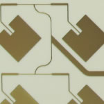
Rogers 4350B |
|
Rogers 4350,Rogers 4003 Manufacturing |
| Rogers 4350B |
|
Rogers 4350B,4003C PCB Manufacturer |
| Ro4350B |
|
Rogers High Frequency PCB Manufaturing China |
Turnkey Services |
|
Turnkey PCB Assembly Services, |
| Turnkey services |
|
Print circuit board Manufacturing, Turnkey Services |
| Turnkey Assembly |
|
Through Hole PCB components wave soldering Assembly |
Aircraft array camera Aluminum mcpcb aplication
-
Aircraft array camera Aluminum mcpcb aplication
The ability to resolve multiple fluorescent emissions from different biological targets in video rate applications, such as endoscopy and intraoperative imaging, has traditionally been limited by the use of filter-based imaging systems. Hyperspectral imaging (HSI) facilitates the detection of both spatial and spectral information in a single data acquisition, however, instrumentation for HSI is typically complex, bulky and expensive. We sought to overcome these limitations using a novel robust and low cost HSI camera based on a spectrally resolved detector array (SRDA). We integrated this HSI camera into a wide-field reflectance-based imaging system operating in the near-infrared range to assess the suitability for in vivo imaging of exogenous fluorescent contrast agents. Using this fluorescence HSI (fHSI) system, we were able to accurately resolve the presence and concentration of at least 7 fluorescent dyes in solution. We also demonstrate high spectral unmixing precision, signal linearity with dye concentration and at depth in tissue mimicking phantoms, and delineate 4 fluorescent dyes in vivo. Our approach, including statistical background removal, could be directly generalised to broader spectral ranges, for example, to resolve tissue reflectance or autofluorescence and in future be tailored to video rate applications requiring snapshot HSI data acquisition.
1 Introduction
HyperSpectral Imaging (HSI) is a powerful analytical tool based on the detection of both spatial and spectral information within a single data set, referred to as a HSI cube (x-y-λ). Originally conceived for remote sensing [1], HSI has impacted fields as diverse as food inspection [2] and forensics [3]. The power of HSI lies in the ability to determine the chemical composition of a sample based on characteristic spectral signatures, using multivariate statistical methods to produce a spatial map of the chemical constituents.
The ability to detect multiple fluorescent labels targeted to different processes is highly advantageous across a range of length scales in biomedical imaging: from studying complex molecular interactions in cells at super-resolution [4]; through monitoring contrast agent biodistribution in small animals [5, 6]; to diagnosing, characterising and resecting cancer in humans [7, 8]. Biomedical application of HSI has already enabled numerous fluorescent contrast sources (e. g. small molecule dyes, fluorescent proteins, autofluorescence) to be delineated within a single data set. Implementations of fluorescence HSI (fHSI) systems in microscopic [9] and small animal imaging [10, 11] based on tunable spectral filters have gained commercial traction [12, 13], however, in practice these systems are typically used to resolve fewer than 3 fluorescent dyes or proteins [9, 14-17]. Increasing the number of resolvable labels to >5 has required the use of narrowband emitters such as quantum dots [18] or specialized sample geometry [19].
Figure 1. Open FigureDownload Powerpoint slide
Characterization of the hyperspectral imaging (HSI) camera. (A) The HSI camera contains a CMOS sensor with row-wise deposition of Fabry-Pérot etalon cavities (simplified schematic); each ‘spectral band’ occupies 8 pixel rows. (B) Experimental setup for calibration. (C) The calibration procedure located 72 spectral bands with peak wavelength between 600 and 900 nm; here shown for a camera objective F/# of 1.65. (D) The quantum efficiency as a function of wavelength – QE(λ) – for each of the 72 spectral bands. As the F/# of the coupled camera objective increases, the total signal falling on the sensor decreases (E), whilst the full width at half maximum (FWHM) narrows (F) differing notably from the QE(λ) collimated light (F, dashed line). Data in (E) and (F) are taken from spectral band 32.
To date, translating the power of fHSI into applications in humans, such as endoscopic and intra-operative imaging, has been challenging due to the need for complex, bulky and expensive instrumentation with limited frame rate. Nonetheless, the ability to characterize both endogenous tissue contrast based on diffuse reflectance and to identify the presence and concentration of exogenous small molecule fluorescent dyes [17, 20] is highly desirable in the clinic.
We “Elenetic Electronics” are actively committed to manufacturing a remarkable array of Single Sided PCB, Printed Circuit Board, PCB Panel, PCB Board, etc. We are a Sole Proprietorship company that is incepted with an aim of providing an excellent quality range of products. Apart from this, we also impart highly reliable PCB Assembling Work and PCB Design And Cam Work. Founded in the year 2015 at Gandhinagar (Gujarat, India), we are providing a high-quality range of products as per the current market needs. Under the direction of our mentor “Mr. Jigar Patel”, we have reached the pinnacle of success.
A poster session will be held on Monday 17.45 to 19.15. Posters will be on display after 10.00 Monday morning in the Conference Centre. Conference attendees are invited to attend the Photonics Europe poster session on Monday. Come view the posters, enjoy light refreshments, ask questions, and network with colleagues in your field. Authors of poster papers will be present to answer questions concerning their papers. Attendees are required to wear their conference registration badges to the poster sessions. Poster authors, view poster presentation guidelines and set-up instructions at
1. IntroductionFor the enhancement of efficiency and life of LEDs, heatproblem is obviously a key issue. Most researches focus on theLED packages, heat sink design, and LED thermal management.Park et al. [1] measured the temperature profiles of the visible LEDchips by the nematic liquid crystal measurement with IR laserillumination. The junction is important for the LED performance.Therefore, the cooling methods of the high power LED array areproposed with focus on the external heat removal system such asheat pipe proposed by Kim et al. [2] and the air cooling system byJane and Shin [3]. The numerical models are proposed sequentiallyfor building the thermal science of LEDs. Hu et al. [4] processed thethermal analysis of the LED package by the transient thermalmeasurement and the thermo-mechanical simulation. The ther-mal resistor network model is proposed by Christensen andGraham [5] and combined with the finite element method topredict the temperature in the system and die level. Chen et al.proposed the compact thermal models of single-chip and multi-chip LED package based on the finite volume simulation whichagree with the experiment [6]. Weng proposed the FEM modelingtechnique to build the LED package with different heat slug, PCB,cooling condition and chip size [7]. Cheng et al. [8] proposedoptimization of multiple LED package using general analytica
Collimator Street Lens , LED Street Light Retrofit Kits For Road Light
Place of Origin:Shenzhen,China
Brand Name:Sunshineopto
Model Number:SUN-LD6X1
Collimator Street Lens , LED Street Light Retrofit Kits For Road Light Quick Detail: 1. Lens Material: optical PMMA 2. Lens Beam Angle :40x80degree 3. Lens size:160.5x26x4.15mm 4. ...
Sunshine Opto-electronics Enterprise Co.,ltd
Verified Supplier
Guangdong
Contact Now
The Golden DRAGONPackage is the newest member of the OSRAM SMT package family. The Golden DRAGONLED consists of a leadframe with integrated heat spreader and a thermoplastic body.The chip is mounted in a reflector formed by the thermoplastic. In order to dissipate the heat the package has an additional thermal connection. This connection is soldered to a thermal enhanced PCB, on the backside of the housing. Therefore the Golden DRAGONpackage is suitable for high power dissipations in the range of 1 W. In order to achieve reliability and optimal performance a proper thermal management design is absolutely necessary. Like all electronic components, the Golden DRAGONLED’s have thermal limitations. The allowed operation temperature for the specific lifetime is limited by the glass-point of the LED resin. This means that the temperature of the die inside, doesn’t have to exceed this value when exposed to the expected operation temperature. This brief will give the design engineer an introduction in the thermal basic of Golden DRAGONLED’s. Furthermore some concepts are shown in order to improve the thermal design
Add To Cart
Optical Collimator Led Street Light Lens Bridgelux chip for Road Lighting Components
Place of Origin:Shenzhen,China
Brand Name:Sunshineopto
Model Number:SUN-LD6X1
Optical Collimator Led Street Light Lens Bridgelux chip for Road Lighting Components Quick Detail: 1. Lens Material: optical PMMA 2. Lens Beam Angle :40x80degree 3. Lens size:160...
Sunshine Opto-electronics Enterprise Co.,ltd
Verified Supplier
Guangdong
Contact Now
High power light-emitting diodes (LEDs) are penetrating into anumber of lightingapplications due to their excellent color saturationand long life characteristics, replacing other technologies such asincandescent and
fl
uorescent bulbs in various lighting solutionsincluding indoor lighting, street lamps, advertising display, backlightsfor LCD TV, traf
fi
c lights, and decorative lighting. LEDs that use from500 mW to as much as 10 W in a single package have becomestandard, and researchers expect that even more power will be usedin the future. The luminous ef
fi
ciency of LEDs has also risen to acertain level in response to the applications. At
fi
rst, gains were madein ef
fi
ciency so that 20 lm/W was achieved quickly. Ef
fi
ciency hasslowly risen in the last few years to around 100 lm/W, and trendsindicate 150 lm/W and higher will occur in the next few years.Both optical extraction and thermal management are critical toguarantee the reliability of LED packaging of modern high brightnessLEDs[1]. Generally,most of the electronic power ~85% of LEDs will beconvertedintoheatandthisheatwillgreatlyreducetheluminosityof the device. In addition, the high junction temperature will shift thepeak wavelength of the LED, which will change the color of the light.Narendran and Gu[2]have experimentally demonstrated that the lifeof LEDs decreases in an exponential manner as junction temperatureincreases. Therefore, a low-operation temperature is essential forLEDs.Mostpracticalsituations requirethatLEDshavehighpoweranddense packaging, but this poses a contradiction between powerdensity and operation temperature, especially when applicationsrequire LEDs to operate at full power to produce the desiredbrightness.In order to improve the performance of the unit LED package, orLEDs array system, metal core printed circuit boards (MCPCBs) arenormally used as the common boards for heat dissipation as theseincorporatea basemetalmaterial,whichactsasa heatspreader,asanintegral part of the circuit board. The metal core is usually made of aluminium alloy. Furthermore these MCPCBs can take advantage of incorporating a dielectric polymer layer with high thermal conduc-tivity for lower thermal resistance. However, due to a lower materialcost, FR4 PCB is still commonly used with high brightness LEDs. Thethermal performance of a combined LED array with FR4 PCB andMCPCB, under different physical conditions, is a useful combinationwhich needs further investigation.In many cases, the casing of the LED array system needs to beenclosed to keep it dust-proof and water-proof, so a naturalconvection cooling scheme might be the only remaining feasibleoption. This is particularly true when it is operating in a position witha varyingangle ofinclination.Forexample,it isnowpossibleto orienttheLEDpanelsinanydirectionsbytheadjustablebracketsystem(seeFig. 1a). This system is designed to illuminate a speci
fi
ed street regionthrough changing the angle of the panel. However, previousinvestigation into the natural heat transfer focuses mainly on thehorizontal and vertical plates. The research so far on natural heattransfer of inclined plate with heat sources on different angles[3,4]isstill lacking. To design an effective cooling system in a closed LEDsarray system and obtain an optimum cooling performance, thebehaviour of natural convection in such a system requires specialconsideration
Hameed Khan, Steve Tessendorf, James Fisher
Acoustical and Thermal treatments for automotive applications are constructed using a number of different materials and composites. These range from the simple needled felt absorber, to the sophisticated multi layer composites to provide noise and thermal Improvements. Since, in most cases a finish fabric or treatment typically covers these materials, the actual color of these substrates has not really been a key design criteria. This has allowed the Acoustics Integrators, when the function of the part is not compromised, to utilize recycled, and byproduct materials. These materials often provide superior performance, lighter weight, and reduced cost from the use of virgin materials. This model of Source Reduction for Acoustical and Thermal Product Design supports the environmentally sustainable Eco system. The End of Life directive may open up more recycled material streams by providing the necessary infrastructure to recover and process the automotive materials.
Thomas O. Leimkuehler, Ryan A. Stephan
Sublimators have been used for heat rejection for a variety of space applications including the Apollo Lunar Module and the Extravehicular Mobility Unit (EMU). Some of the attractive features of sublimators are that they are compact, lightweight, and self-regulating. One of the drawbacks to previous designs has been sensitivity to non-volatile contamination in the feedwater, which can clog relatively small pores (∼3-µ6 μn) in the porous plates where ice forms and sublimates. The Contaminant Insensitive Sublimator (CIS) has been recently developed at NASA-JSC to be less sensitive to contaminants by using a larger pore size media (−350 um). Testing of a CIS Engineering Development Unit (EDU) has demonstrated good heat rejection performance. This paper describes testing that investigates different factors affecting efficient utilization of the feedwater.
Power integrity (PI) has become a limiting factor for the chip's overall performance, and how to place in-package decoupling capacitors to improve a chip's PI performance has become a hot issue. In this paper, we propose an improved transmission matrix method (TMM) for fast decoupling capacitance allocation. An irregular grid partition mechanism is proposed, which helps speed up the impedance computation and complies better with the irregular power/ground (P/G) plane or planes with many vias and decoupling capacitors. Furthermore, we also ameliorate the computation procedure of the impedance matrix whenever decoupling capacitors are inserted or removed at specific ports. With the fast computation of impedance change, in-package decoupling capacitor allocation is done with an efficient change based method in the frequency domain. Experimental results show that our approach can gain about 5× speedup compared with a general TMM, and is efficient in restraining the noise on the P/G plane.
The GeoSteiner software package for computing Steiner trees in the plane
DEFF Research Database (Denmark)
Juhl, Daniel; Warme, David M.; Winter, Pawel;
The GeoSteiner software package has for more than 10 years been the fastest (publicly available) program for computing exact solutions to Steiner tree problems in the plane. The computational study by Warme, Winter and Zachariasen, published in 2000, documented the performance of the Geo......Steiner approach --- allowing the exact solution of Steiner tree problems with more than a thousand terminals. Since then, a number of algorithmic enhancements have improved the performance of the software package significantly. In this computational study we run the current code on the largest problem instances...... from the 2000-study, and on a number of larger problem instances. The computational study is performed using both the publicly available GeoSteiner 3.1 code base, and the commercial GeoSteiner 4.0 code base....
RNA structure. Structure of the HIV-1 RNA packaging signal.
Add To Cart
Led Street Light Module with Bridgelux Led Lens ,Aluminum PCB mounting leds
Place of Origin:Shenzhen,China
Brand Name:Sunshineopto
Model Number:SUN-LD6X1
Led Street Light Module with Bridgelux Led Lens , Aluminum PCB mounting leds Quick Detail: 1. Lens Material: optical PMMA 2. Lens Beam Angle :40x80degree 3. Lens size:160.5x26x4...
Sunshine Opto-electronics Enterprise Co.,ltd
Verified Supplier
Guangdong
Contact Now
Full Text Available Retroviruses can cause diseases such as AIDS, leukemia and tumors, but are also used as vectors for human gene therapy. All retroviruses, except foamy viruses, package two copies of unspliced genomic RNA into their progeny viruses. Understanding the molecular mechanisms of retroviral genome packaging will aid the design of new anti-retroviral drugs targeting the packaging process and improve the efficacy of retroviral vectors. Retroviral genomes have to be specifically recognized by the cognate nucleocapsid (NC domain of the Gag polyprotein from among an excess of cellular and spliced viral mRNA. Extensive virological and structural studies have revealed how retroviral genomic RNA is selectively packaged into the viral particles. The genomic area responsible for the packaging is generally located in the 5’ untranslated region (5’ UTR, and contains dimerization site(s. Recent studies have shown that retroviral genome packaging is modulated by structural changes of RNA at the 5’ UTR accompanied by the dimerization. In this review, we focus on three representative retroviruses, Moloney murine leukemia virus (MoMLV, human immunodeficiency virus type 1 (HIV-1 and 2 (HIV-2, and describe the molecular mechanism of retroviral genome packaging.
Abstract
Abstract | Introduction | Experimental Methodology | Thermal Modeling | Formulation of the Placement Method and Examples | Results and Discussion | Conclusion | Acknowledgements | References
This paper reports the thermal performance of a high-brightness light-emitting diode (LED) array package with a novel placement method on a printed circuit board (PCB). The precise heat transfer analysis and modeling using computational fluid dynamics (CFD) were performed according to the practical working conditions of the LED array. Emphasis was placed upon investigating how the temperature of the surface of LEDs changed in accordance with different placement methods. A significant drop in the surface temperature of the LEDs was found when the triangular and arithmetic spacing placement methods were used; hence, the overall heat dissipating capability of the LED array to the PCB was improved. By optimizing the placement design, the average surface temperature of the LED array achieved a decrease of about 20%, from 120°C120°C to 100°C100°C. The illuminance level of each placement design was measured and compared. Both CFD simulation and experimental results are provided to demonstrate the efficacy of the proposed approach for LED array thermal management.
Spectrally resolved detector arrays (SRDAs) – where the spectral filters are deposited on a glass substrate either in front of [21, 22], or directly on top of, the sensor array [23, 24] – are promising for future clinical application of fHSI. SRDAs are extremely compact and robust and therefore well suited for use in an endoscopy suite or operating theatre. They also have the potential to be produced at very low cost, as the filters may be deposited on the sensor array during the lithography process [23]. When the spectral filters are deposited on the sensor in a pixel-wise mosaic pattern, video rate spectral imaging is possible [24]. Encouragingly, early applications of snapshot SRDA have shown promise in neurosurgery [25] and ophthalmology [26] using white-light reflectance imaging.
Imaging in the long wavelength infrared (LWIR) range from 8 to 14 μm is an extremely useful tool for non-contact measurement and imaging of temperature in many industrial, automotive and security applications. However, the cost of the infrared (IR) imaging components has to be significantly reduced to make IR imaging a viable technology for many cost-sensitive applications. This paper demonstrates new and improved fabrication and packaging technologies for next-generation IR imaging detectors based on uncooled IR bolometer focal plane arrays. The proposed technologies include very large scale heterogeneous integration for combining high-performance, SiGe quantum-well bolometers with electronic integrated read-out circuits and CMOS compatible wafer-level vacuum packing. The fabrication and characterization of bolometers with a pitch of 25 μm × 25 μm that are arranged on read-out-wafers in arrays with 320 × 240 pixels are presented. The bolometers contain a multi-layer quantum well SiGe thermistor with a temperature coefficient of resistance of -3.0%/K. The proposed CMOS compatible wafer-level vacuum packaging technology uses Cu-Sn solid-liquid interdiffusion (SLID) bonding. The presented technologies are suitable for implementation in cost-efficient fabless business models with the potential to bring about the cost reduction needed to enable low-cost IR imaging products for industrial, security and automotive applications.
Here, we evaluated the performance of an SRDA-based HSI camera for fluorescence imaging, with a view to future clinical application. While the SRDA filters can be deposited pixel-wise for real-time ‘snapshot’ imaging [24-26], we used row-wise filters to perform ‘pushbroom’ HSI in order to maintain high spatial and spectral resolution in this initial technology evaluation. The utility of the ‘pushbroom’ SRDA used in this study has been explored in a wide range of applications, from food inspection to agricultural monitoring [27]. Following detailed characterization of the HSI camera, we created a reflectance-based wide-field imaging system in order to provide a first proof-of-concept for fHSI using an SRDA. We evaluated: HSI response linearity; spectral unmixing precision; and delineation of reflectance and fluorescence light in tissue. The wide-field fHSI system based on our SRDA can resolve at least 7 fluorescent dyes in solution and at least 4 in small animals, showing promising performance for future clinical application.
ISO 9001:2008 & AS 9100C certified and NADCAP AC7120 accredited contract electronics manufacturer of advanced printed circuit board, printed wiring board and circuit card assemblies for commercial, industrial and military applications. Quick-turn rapid prototypes and production volumes. SBA certified woman-owned small business (WOSB). Made in Connecticut. Rigid, flex, rigid-flex, ceramic, aluminum metal core (MCPCB), SMT, PTH, BGA, uBGA, 0201, 10mil pitch. Ionic chromatography laboratory for cleanliness testing and robotic hot solder dipping (RHSD) component preparation. DFM/DFT, AOI, x-ray & MDA/ICT testing. Parylene, silicone, urethane, epoxy and acrylic coatings. Staking, underfill, potting & encapsulation. Full lot code control & traceability with counterfeit parts mitigation. RoHS & REACH compliant.
www.techmfgcorp.com/boards.html
AcHmed99:
1k lumen is pretty bright if i remember right the 100w incadesence is around 1600lumen total. the led emits around 115 and 130degrees from its base its damn bright
The increasing demand for light emitting diodes (LEDs) has been driven by a number of application categories, including display backlighting, communications, medical services, signage, and general illumination. The construction of LEDs is somewhat similar to microelectronics, but there are functional requirements, materials, and interfaces in LEDs that make their failure modes and mechanisms unique. This paper presents a comprehensive review for industry and academic research on LED failure mechanisms and reliability to help LED developers and end-product manufacturers focus resources in an effective manner. The focus is on the reliability of LEDs at the die and package levels. The reliability information provided by the LED manufacturers is not at a mature enough stage to be useful to most consumers and end-product manufacturers. This paper provides the groundwork for an understanding of the reliability issues of LEDs across the supply chain. We provide an introduction to LEDs and present the key industries that use LEDs and LED applications. The construction details and fabrication steps of LEDs as they relate to failure mechanisms and reliability are discussed next. We then categorize LED failures into thirteen different groups related to semiconductor, interconnect, and package reliability issues. We then identify the relationships between failure causes and their associated mechanisms, issues in thermal standardization, and critical areas of investigation and development in LED technology and reliability.
i made this little panel with 14 luxeon rebel leds these ones mounted supposed to be 160lumens each at 700ma drive current. they pretty damn bright and heats up quickly, f***d up the thermal plane in the middle either too few vias already there is 150 in staggered row configuration or too small diamater ive used 0.5mm vias on 1oz copper with an 1.6mm fr4 had to solder the bottom 2 mounting holes trough into the aluminium heatsink to bring the leds base to 50celsius at 700ma drive. i wonder btw if tripled amount of vias would be good as i dont like the perforated example design for these leds 30+ vias at the base of the led... or would be simply solved by an aluminium core pcb. but i would simply wticht to 1 of those vero arrays instead as these small leds whati have only 76lumen/w and the vero arrays are at 110+. make another batch of these boards would not worth for me as i didnt paid more for 50 of these leds then for the 10pcs 10x5cm boards
sorry for the pciture quality taken by a 6300 in low light conditions as i couldnt find the digital camera when i took the picture
For furhter information, please feel free to contact us, www.pcbsino.com