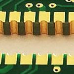
WHigh power current converter Aluminum mcpcb aplication
China PCB Manufacturing, Shenzhen PCB Manufacturer, Making Circuit boards
PCB Contract manufacturer, PCB Fabrication, Turnkey assembly services
Buy Print circuit board, customer: /USA/UK/Canada/South Africa...
PCB Supplier Shenzhen, China, PCB Manufacturer, Turnkey services
-
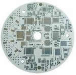
PCBSINO is the Top 5 PCB manufacturer company in China.
PCBSINO do rapid Prototype within 24 hours. our rigid PCB like MCPCB and Rogers PCB, FR4, High TG FR4, Rogers 4003, 4350,Al Aluminum metal Core MCPCB, Al2O3 Ceramic,Taconic,Halogen Free material, CEM-3, Fr2, CEM-1, CEM-2, 94VO, Rogers HF material, Polymide, etc.
PCBSINO making many type electronic product for our customer, Our turkey services team can source original components part for your project(Digikey/Mouser/RS...), senior Electronic engineer will follow each step of the production to solve any PCB problem and our team will do final function test in PCB house.
Express PCB |
|
Rigid PCB Rapid Prototype,24 hours |
| Fr4 PCB |
|
prototype Lower to 15USD ! |
| Rapid Prototype |
|
Fr4 Rigid PCB Rapid Prototype China, |
MCPCB |
|
MCPCB Manufacturer China, Shenzhen |
| Aluminum PCB: |
|
Aluminum Metal Core PCB manufacturing, Fabrication |
| Aluminum PCB: |
|
single side, double side MCPCB, 0.5-5mm or more |
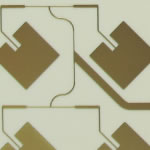
Rogers 4350B |
|
Rogers 4350,Rogers 4003 Manufacturing |
| Rogers 4350B |
|
Rogers 4350B,4003C PCB Manufacturer |
| Ro4350B |
|
Rogers High Frequency PCB Manufaturing China |
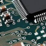
Turnkey Services |
|
Turnkey PCB Assembly Services, |
| Turnkey services |
|
Print circuit board Manufacturing, Turnkey Services |
| Turnkey Assembly |
|
Through Hole PCB components wave soldering Assembly |
WHigh power current converter Aluminum mcpcb aplication
-
WHigh power current converter Aluminum mcpcb aplication
There are many names for these products; Aluminum clad, aluminum base, Metal clad printed Circuit Board (MCPCB), Insulated Metal Substrate(IMS or IMPCB), Thermally conductive PCBs, etc… but they all mean the same thing and perform the same way.
How Are Aluminum PCBs Made?
A thin layer of thermally conductive but electrically insulating dielectric is laminated between a metal base and a copper foil. The copper foil is etched into the desired circuit pattern and the metal base draws heat away from this circuit through the thin dielectric.
Benefits of Aluminum PCBs
Heat dissipation is dramatically superior to standard FR-4 constructions.
The dielectrics used are typically 5 to 10 times as thermally conductive as conventional epoxy-glass and a tenth of the thickness
Thermal transfer exponentially more efficient than a conventional rigid PCB.
Lower copper weights than suggested by the IPC heat-rise charts can be used.
THERMAL CLAD & METAL BACKED PRINTED CIRCUIT BOARDS
Reada offers thermal clad and metal printed circuit boards with a full selection of high performance or low cost materials from leading suppliers around the world. Thermal clad PCB's are a dielectric metal base with a bonded copper circuit layer. This creates superior heat transfer to help cool components while eliminating problems associated with managing fragile ceramics.
With a wide range of electrical and thermally conductive interface pads, thermally conductive gap fillers, thermal phase change materials and thermally conductive electrically insulating materials, we can manufacture thermal clad & metal backed printed circuit boards that exceed all of our customers' expectations.
Thermal Clad Layers
Thermal clad is a unique layered system comprised of the follow layers.
Circuit Layer:
Printed circuit foil with thickness of 1oz to 5 oz.
Dielectric Layer:
Many different options which offer electrical isolation with minimum thermal resistance. Also used to bond the circuit layer and base material together. Each specific dielectric has its own UL recognition.
Base Layer:
Most often Aluminum, but can also be copper. The most commonly used thickness iThermal clad is a unique layered system comprised of the follow layers.
Thermal Clad substrates minimize thermal impedance and conduct heat more effectively and efficiently than standard printed wiring boards (PWB's). These substrates are more mechanically robust than thick-film ceramics and direct bond copper constructions that are often used in these applications.
Thermal Clad is a cost-effective solution which can eliminate components, allow for simplified designs, smaller devices and an overall less complicated production processes. Additional benefits of Thermal Clad include lower operating temperatures, longer component life and increased durability.
Henkel Thermal Clad substrates are not limited to use with metal base layers. In one example, power conversion applications can enhance their performance by replacing FR-4 with Thermal Clad dielectrics in multi-layer assemblies. In this application, the thickness of the copper circuit layer can be minimized by the high thermal performance of Thermal Clad. For additional information on this topic, refer to the “Specialty Applications” section on pages 10-11 of this guide.
A simple layer single sided MCPCB consists of a metal base (usually aluminum, or copper alloy), Dielectric (non-conducting) Layer, Copper Circuit Layer, IC components and solder mask.
The prepreg dielectric provides excellent heat transfer from the foil and components to the base plate, while maintaining excellent electrical isolation. The base aluminum/copper plate gives the single-sided substrate mechanical integrity, and distributes and transfers the heat to a heat sink, mounting surface or directly to the ambient air.
The Single-Layer MCPCB can be used with surface mount and chip & wire components, and provides much lower thermal resistance than FR4 PWB. The metal core provides lower cost than ceramic substrates, and allows much larger areas than ceramic substrates.
Double Layers Metal Core PCB
Double layers MCPCB is consisting of two layers of copper conductor, put them on same side of metal core (usually aluminum, copper or iron alloy). The metal base is on the bottom of whole MCPCB, which is different from double sided MCPCB(the two copper layers were put on the each side of metal core respectively), and you can only populate SMD on top side.
Different with Single layer MCPCB, 2 layers MCPCB requires an additional pressing step to laminate the imaged thermal conductive laminate and metal core (also known as metal base) together.
Compared with normal FR4, this sturcture need more technology and experience on laminating of two layers together with metal core.
The processing steps of the MCPCB with the metal base embedded in the PCB are comparatively complex as hole plugging is required after primary drilling on the metal base in order to isolate it from the circuitry.
Double Sided Metal Core PCB
It also has same two layers of copper conductor like Double layers MCPCB, but the metal core is in the middle of two conductor, so there're conductors (trace) on both sides of metal core, and were connected to each other by Vias. So we named it "Double sided MCPCB", and you can populated SMD on both top and bottom.
Different with Single layer MCPCB, double sided MCPCB also requires an additional pressing step to laminate the imaged thermal conductive laminate and metal core (also known as metal base) together. But sometimes, some raw Metal Clad material vendor will supply board material which already laminated.
Compared with normal FR4, this sturcture need more technology and experience on laminating of two layers together with metal core.
The prototype design was developed based on commercially available HBLEDs. First, a numerical CFD model was developed to predict the reduction in PCB thermal resistance that could be attained with the addition of low evaporative resistance heat pipes. Secondly, an experimental investigation was carried out to validate modeling, and examine the various designs for ease of manufacturability.
3.1 CFD Modeling Predictions
The modeling results are shown in Figure 3. The temperature difference, ΔT, is defined as the peak temperature on the heat input side of the PCB minus the average temperature on the heat sink side. The heat load Qin was applied to a pad similar to the size of the footprint of the selected LED, and pin finned heat sink with forced air cooling is applied to the back side.
High brightness LEDs (HBLEDs) are finding increasing usage in applications like high bay lighting, theatrical stage lighting, and UV curing among others. A typical HBLED chip has a 1mm2 mounting surface area and a total power consumption of 1 Watt. According to the power to heat conversion rate of 70 – 80%, the heat flux can be as high as 80 W/cm2. In the next few years, that heat flux is expected to increase to over 300W/cm2 in some applications, which is 6-7 times higher than that of convectional CPU chips [2]. The high junction level heat fluxes, coupled with dense packaging, results in two thermal management challenges: temperature uniformity across multiple LED junctions and in-plane heat spreading at the heat sink and PCB package levels. The state of-the-art thermal solutions for LED applications most often relies on conduction through low thermal conductivity thermal interface materials to solid Aluminum heat sinks, which are becoming inadequate at dissipating the increasingheat fluxes.
To date, many heat dissipation solutions have been investigated for the thermal management of high-power LEDs, from the chip package level to the printed circuit board (PCB) level to the system level. The package level thermal management research, which involves thermal material research, package design optimization, and LED array optimization, are important to determine the package thermal resistance [3, 4, 5, 6]. The board-level thermal management research is mainly focused on solder material, bonding method improvement, and printed circuit board design optimization [7, 8, 9, 10, 11]. On the system level, fin-heat sinks with external active cooling is still the mainstream method in industry due to its high reliability and lowest cost [5].
The use of sophisticated PCBs based on FR4 and copper with partially embedded copper elements allows for powerful thermal management as well as a simple way of combining complex control electronics with sensors on the LED board. HSMtec makes it possible to realize the fine structures required for the control electronic simply on the same layer as the copper elements without any additional design tools.
HSMtec for Zhaga Compliant Spotlights
Zhaga certified “LED-Light-Engines” are rather complex: While the standardization applies to the LED module, Zhaga distinguishes between modules with and without a driver supplying the operation current. Both variants already have their own standard for example defining the module’s size, its external diameter and its height.
These standardization efforts pose enormous challenges for PCB manufacturers and luminaire designers. A typical Zhaga compliant spot light engine couples out light on an area measuring 13.5 to 26mm in diameter. The resulting high power density requires a very efficient thermal management. On the other hand, a LED module with integrated driver has to cope with 230V input voltage and ensure an dieelectric strength conforming to standards as well as electric isolation.
There isn’t much space left in the socket for multiple PCBs for LEDs and their control electronics. Usually, IMS boards are being used in order to dissipate the heat generated by the LEDs. This method requires cables and connectors to connect the LED board with a second FR4-based one containing the control electronics. There is no question that this configuration is not ideal, impairing life expectancy of the module and luminance of the LEDs.
This is where HSMtec demonstrates its advantages: A LED cluster measuring 19 mm in diameter with 30 Cree XLamp LEDs type XB-D and a total power of 100 W acts as reference module. It conforms to the intended Zhaga performance goals of 50 W per module with integrated driver without difficulty, and control electronics can be mounted on the same board as the driver components.
A field-proven module is a 28 mm by 28 mm LED array with 33 Cree XLamp XP-E-RGB high-brightness LEDs with 2W each. It uses a 4-layer HSMtec FR4 multilayer and is being used in the LED floodlight SpectraWow+ from LDDE which is supposed to redefine additive color mixing. The result is a functional floodlight for stage lighting and architectural lighting with integrated RGB color mixing. The headlight uses a high-power engine as RGB version but is available also with white light with 3200K and 5700K color temperature. Combined with a special honeycomb lens, the floodlight shines very uniformly. Furthermore, undesirable color shadows, common in many LED headlights with single-lens optics, are a problem of the past.
In this paper, an advanced high-power LED cooling technology targeted at reducing the thermal resistance on the PCB level is presented. This technology integrates passive two-phase heat pipe technology into a metal core printed circuit board, which effectively converts the PCB into a higher performance heat spreader. Although other two-phase heat pipe technologies have been investigated by other groups [10, 12], the novelty of the current concept involves an exceptionally low thermal resistance heat pipe wick structure that is capable of achieving very low thermal resistances while maintaining high heat transport capabilities. Thus the new design can significantly enhance cooling, which allows the LED to run at higher fluxes without degradation in performance, as well as improve heat spreading that is particularly effective in cooling arrays of high density chips.
For the CFD model setup, an effective heat sink resistance of 0.3°C/W was applied to the entire backside of the MCPCB, which is consistent with a reasonably sized pin fin heat sink with forced air convection. The overall size of the MCPCB measured 27cm2, which is consistent with common MCPCB sizes associated with high power LED applications. A heat source positioned on center, measuring 0.27cm2 was specified at 30 Watts, which resulted in a input heat flux of ~110 W/cm2. All other surfaces were assumed to be adiabatic. Base material was 6061 Aluminum and heat pipe modeling parameters were consistent with the researcher’s standard heat pipe modeling practice.
The CFD analysis shows that the evaporative heat transfer efficiency of the heat pipe plays a critical role in overall thermal performance of the heat pipe embedded MCPCB. Results suggest that the evaporative heat transfer coefficients typical of standard wire mesh heat pipe wick structures maybe inadequate due to the small heat input area of the LED, and consequently a high heat flux. This theory is consistent with experimental data presented in the subsequent section on Experimental Heat Pipe Embedded MCPCBs
These types of PCBs are also called aluminum base, aluminium PCBs, aluminum clad, insulated metal substrate (IMS), metal clad (MCPCB), or thermally conductive PCBs.
For a typical metal based single sided PCB, the base laminate is made up of copper foil bonded to a thin thermally conductive insulating dielectric which is in turn bonded to a thick metal base, usually aluminium. The copper layer is processed in the normal way to create the tracking layer, and the profile is machined to the required shape and size. The aluminium substrate must be protected from the etching chemicals during the manufacturing process.
The material is particularly suited for population with surface mounted devices. Through hole components are not appropriate because the metal base material is not an insulator. We only offer single sided metal clad PCBs.
Why use Aluminium based copper clad PCBs?
Greatly improved heat dissipation without using external heat-sinks
Very mechanically rigid base laminate
Dramatically reduce thermal stress on components, improving reliability and MTBF
Relatively low cost
Improved heat transfer allows thinner base copper and thinner tracking for high current designs as compared with standard FR4 laminate PCB construction
Better thermal management permits closer component mounting and smaller PCBs, yielding overall cost savings
Multi Layers Metal Core PCB
Just like FR4 PCB, we can also make boards with more than 2 layers of traces and we named it "Multi Layers MCPCB". The structure is similar with FR4 Multi Layers, but it much more complex to make.
You can populated more components on the boards, put signal and ground layer into seperated layers, to achieve better performance in electrical performance.
Compared with normal FR4, this sturcture need more technology and experience on laminating of more than two layers together with metal core and the cost is much higher than 2 layers MCPCBor double sided MCPCB.
Traditionally, cooling an FR-4 board required use of a large heat sink, interface material and various hardware (brackets, screws or clamps); a configuration requiring labor intensive manual assembly.
Cooling with Thermal Clad can eliminate the need for heat sinks, device clips, cooling fans and other hardware. An automated assembly method will reduce long term costs.
Circuit Layer:
Printed circuit foil with thickness of 1oz to 5 oz.
Dielectric Layer:
Many different options which offer electrical isolation with minimum thermal resistance. Also used to bond the circuit layer and base material together. Each specific dielectric has its own UL recognition.
Base Layer:
Most often Aluminum, but can also be copper. The most commonly used thickn although many thicknesses are available.
s 0.040" (1.0mm) although many thicknesses are available.
Applications of Aluminum PCBs
Although Power Converters and LEDs are the largest users of these products, Automotive and RF companies are also looking to take advantage of the benefits of these constructions. While a single layer construction is the simplest, other configuration options are available at Amitron, including:
Flexible Aluminum PCBs
One of the newest developments in IMS materials is flexible dielectrics. These materials feature a polyimide resin system with ceramic fillers which provides excellent electrical insulation, flexibility and of course thermal conductivity. When applied to a flexible aluminum material like 5754 or similar, the product can be formed to achieve a variety of shapes and angles which can eliminate costly fixtures, cables and connectors. Although these materials are flexible, they are intended to be bent into place and remain in place. They are not suited for applications that are intended to be flexed regularly.
For furhter information, please feel free to contact us, www.pcbsino.com