IPC-2221B Flex PCB application
China Flex PCB Manufacturing, Shenzhen Flex PCB Manufacturer, Making Flex Circuit boards
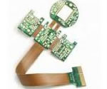
Flex PCB Contract manufacturer, PCB Fabrication, Turnkey assembly services
Buy Flexible Print circuit board, customer: /USA/UK/Canada/South Africa...
Flex PCB Supplier Shenzhen, China, Flex PCB Manufacturer, Turnkey services
-
PCBSINO is the Top 5 PCB manufacturer company in China.
PCBSINO do rapid Flexible PCB Prototype within. we can make Flexible Print circuit boards and Rigid circuit boards, Flex and Rigid Flex PCB, single side, double side, multilayer Flexible print circuit board
PCBSINO making many type electronic product for our customer, Our turkey services team can source original components part for your project(Digikey/Mouser/RS...), senior Electronic engineer will follow each step of the production to solve any PCB problem and our team will do final function test in PCB house.
Flex PCB |
|
Rigid FlexPCB Rapid Prototype |
| Flex PCB |
|
prototype of Flex PCB |
| Flex Prototype |
|
Rigid-Flex PCB Rapid Prototype China, |
Turnkey Services |
|
Turnkey Flex PCB Assembly Services, |
| PCB assembly |
|
Print circuit board Manufacturing, Turnkey assembly |
| PCBA Assembly |
|
SMT Assembly, EMS/OEM supplier China |
IPC-2221B Flex PCB application
-
IPC-2221B Flex PCB application
Using a tutorial based on best practices developed by experts with volunteers who together have hundreds of years’ experience, also makes the document easier to use and understand. The tutorial includes a number of tips offered by these subcommittee members. The tutorial also removes from the main body of the document several narrative paragraphs and themes, which helps keep the main document focused primarily on design requirements.
The new version of the standard has also been updated to address technology that has matured in the years since the last revision. IPC-2223C includes plenty of information on adhesiveless materials, which weren’t included in earlier documents. As adhesive quality has improved, many manufacturers have moved away from substrates with adhesives.
“We tried to emphasize adhesiveless materials,” said William Ortloff, chair of the D-11 Flexible Circuits Design Subcommittee. “Adhesiveless materials are better for soldering; they don’t have the lower temperature requirements common to adhesive based substrates, which can cause problems with glues.”
While the standard has new sections, committee members kept its size down by avoiding redundancy. Ortloff noted that the standard focuses on aspects that are distinctly tied to flexible circuitry. Technologies such as blind, buried and microvias that are the same in flex and rigid printed boards aren’t included in IPC-2223C. Instead, users are referred to other standards such as IPC-2221 and IPC-2222 that address these technologies.
There are three Classes of printed boards called out in IPC-6011 that include Class 1 General Electronic Products, Class 2 Dedicated Service Electronic Products and Class 3 High Reliability Electronic Products. Class 1 has the lower requirements and Class 3 with the toughest requirements. There is a new Class called out in IPC-6012, Class 3/A, which includes Space and Military Avionics which is the highest Class for printed circuits. The Class 1, 2 3 and 3/A specifications are called out in IPC-6012 Rigid. The requirements are also found in IPC 6013 Flex, IPC-6014 PCMCIA, IPC-6015 MCM-L, IPC-HF-318 High Frequency, IPC-A-600 and other IPC documents. Since there are four standards Classes 1, 2, 3, and 3/A the most requirements appear to be in the IPC-6012-2010 document as outlined in appendices A and B.
General documents
IPC-T-50 Terms and Definitions
IPC-2615 Printed Board Dimensions and Tolerances
IPC-D-325 Documentation Requirements for Printed Boards
IPC-A-31 Flexible Raw Material Test Pattern
IPC-ET-652 Guidelines and Requirements for Electrical Testing of Unpopulated Printed Boards
Design specifications
IPC-2612 Sectional Requirements for Electronic Diagramming Documentation (Schematic and Logic Descriptions)
IPC-2221 Generic Standard on Printed Board Design
IPC-2223 Sectional Design Standard for Flexible Printed Boards
IPC-7351B Generic Requirements for Surface Mount Design and Land Pattern Standards
Material specifications
IPC-FC-234 Pressure Sensitive Adhesives Assembly Guidelines for Single-Sided and Double-Sided Flexible Printed Circuits
IPC-4562 Metal Foil for Printed Wiring Applications
IPC-4101 Laminate Prepreg Materials Standard for Printed Boards
IPC-4202 Flexible Base Dielectrics for Use in Flexible Printed Circuitry
IPC-4203 Adhesive Coated Dielectric Films for Use as Cover Sheets for Flexible Printed Circuitry and Flexible Adhesive Bonding Films
IPC-4204 Flexible Metal-Clad Dielectrics for Use in Fabrication of Flexible Printed Circuitry
Performance and inspection documents
IPC-A-600 Acceptability of Printed Boards
IPC-A-610 Acceptability of Electronic Assemblies
IPC-6011 Generic Performance Specification for Printed Boards
IPC-6012 Qualification and Performance Specification for Rigid Printed Boards
IPC-6013 Specification for Printed Wiring, Flexible and Rigid-Flex
IPC- 6202 IPC/JPCA Performance Guide Manual for Single- and Double-Sided Flexible Printed Wiring Boards
PAS-62123 Performance Guide Manual for Single & Double Sided Flexible Printed Wiring Boards
IPC-TF-870 Qualification and Performance of Polymer Thick Film Printed Boards
Flex assembly and materials standards
IPC-FA-251 Assembly Guidelines for Single and Double Sided Flexible Printed Circuits
IPC-3406 Guidelines for Electrically Conductive Surface Mount Adhesives
IPC-3408 General Requirements for Anisotropically Conductive Adhesives Films
Clearance and insulation
Calculating Creepage and Clearance Early Avoids Design Problems Later
The Evaluation of Spacings in Electronic Product Design
Calculating spacing between PCB traces for various voltage levels
European standard: EN60065:2002 "Audio, video and similar electronic apparatus. Safety requirements"
IPC standard: IPC-2221A "Generic Standard on Printed Board Design"
Saturn PCB Design Toolkit A free download tool for calculating conductor spacing and other parameters
Current carrying capacity
Articles on Trace Current/Temperature/Power/Resistance
IPC standard: IPC-2152 "Standard for Determining Current Carrying Capacity in Printed Board Design"
Saturn PCB Design Toolkit A free download tool for calculating current carrying capacity and other parameters
Online ANSI IPC-2221A PCB Trace Width Calculator
Impedance calculators
How does NASA Manage PCB Supply Chain Risks?
Risk management processes enable NASA and its printed circuit board supply chain participants, to systematically analyze, communicate, and mitigate the risk of quality, reliability or performance shortfalls. The process requires development of risk mitigation methods and the implementation of approved strategies to reduce or eliminate the likelihood of quality escapes and failures. Some methods that are used by NASA for managing and mitigating supply chain risk include:
1. Identifying the risks (for example, risks related to the use of a particular requirement, standard, material, design, facility or fabrication technique).
2. Assess the risks, analyze to determine risk likelihood (probability) and severity of consequences (impact of degraded performance, for example, interpret the risk due to use of outdated specification, analyze the impact and evaluate the importance of the risk).
3. Conducting failure modes and effects analysis to identify the modes and failure mechanisms that can affect the functionality of a printed circuit board or assembly.
4. Planning and implementing solutions after formulating risk management strategies and determining an acceptable level of risk.
5. Continuous improvement methods that include analyzing re-engineered processes, influencing the specification and standards, benchmarking, tracking, controlling and communicating.
Technical Standards Activities of the NASA Workmanship Program
The NASA Workmanship Program is taking the following actions to develop assurance guidance and requirements that can be applied Agency-wide in the following manner:
1. NASA PCB Working Group
The NASA PCB Working Group is a resource for printed circuit board technology assessment and provides policy recommendations for printed circuit board quality assurance. The group recommends Safety and Mission Assurance requirements for PCBs to the NASA Office of Safety and Mission Assurance via the NASA Workmanship Program. The Working Group also communicates lessons learned technical recommendations and shares observations on new and altered printed circuit board products. The assessments are performed by weighing the impacts on NASA missions and in some cases, sharing test data.
Current issues being discussed by the NASA WG:
· Applicability and use of high density interconnects such as stacked µvias and via-in-pad technology in current hardware
CURRENT STATUS (3/2017): Participating in update to IPC-2226. Reviewing industry data, literature and experiences.
· Discussions of new laminate materials, i.e.: High Tg, low CTE, selection of via fill materials
CURRENT STATUS (3/2017): Reviewing manufacturers’ datasheets and published literature.
· Use of simulated reflow conditions as a method of performing quality screens on coupons containing high density interconnects such as microvias.
CURRENT STATUS (3/2017): Reviewing design and process conditions to determine, on a case-by-case basis, instances where modified preconditioning conditions may apply.
2. Contributions to Industry and NASA Technical Standards
When the Working Group lessons learned or recommendations have a strong potential for systematic risk reduction across all NASA Projects, the Working Group provides related information to standardizing bodies, such as the IPC, in the form of a design rule, material recommendation, or a manufacturing or quality inspection/acceptance requirement. Once published in a technical standard the guidance, requirement, or the standard as a whole, can be referenced and imposed by NASA hardware developers in their procurement contract statements of work, in purchase orders or other procurement vehicles where technical requirements are established.
3. Independent Technical Evaluations
IPC-SPECS:
where k, b, and c are constants resulting from curve fitting to the IPC-2221 curves
Disclaimer:
These calculations are believed to be correct, but not guaranteed. Use at your own risk!
Trace Width Calculator FAQs
QUESTION: Very cool PCB width tool! I would like to know its limits though. I entered a 65 amp current requirement and it returned a track width that must be incorrect.
ANSWER: The original graphs that this tool is based on (published in IPC-2221) only cover up to 35 Amps, up to 0.4 inches of trace width, from 10 to 100 degrees C of temperature rise, and copper of 0.5 to 3 ounces per square foot. The formulas used here will simply extrapolate when the values are outside of these ranges.
QUESTION: I used your PCB trace width calculator. Intuitively I would say the required internal trace width would be less than the external case since the external trace can peal off; the opposite is true according to the calculator???? Why?
ANSWER: In air, the external layers have better heat transfer due to convection. A good heat insulator blankets the internal layers, so they get hotter for a given width and current. Since the Trace Width Calculator tries to control the temperature rise of the traces, it makes the internal traces wider. In vacuum, or in a potted assembly, you should use the internal layer guidelines even for the external layers.
QUESTION: What does temperature rise mean and how does it apply?
Elements Determining Maximum Current Carrying Capacity
Although a simple formula can be directly employed to calculate maximum current carrying capacity, practical cases are not that simple and direct. That's because apart from cross-sectional area and temperature rise, trace current carrying capacity also depends on other elements such as number of components, pad and vias.
For traces with many pads distributed, the tinning trace will perform an extremely higher capacity than ordinary traces. It's not a rare condition in which engineers meet circuit boards on which some trace between pads is burned down as a large current is flowing through. The reason for such tragedy lies in too much solder paste on components or pins leads to an increased cross-sectional area while no modification occurs to trace between pads. As a result, as soon as power starts or order modification is implemented on trace, it's possible to cause a super large transient surge or even burning down of a trace between pads.
“We provided a lot of information that can help designers make decisions between surface finish alternatives,” said John Perry, IPC technical project manager. Perry added that descriptive data within the standard is augmented by a table that makes it easier to quickly compare the traits of various surface finishes.
Industry’s focus on quality and reliability is addressed with an upgraded section on electrical requirement testing. “There are several pages of new material on electrical testing that explain the various types of tests available, including continuity, Hi-Pot and impedance,” Perry said. “Ultimately, the message is that no one test meets all requirements. Designers are encouraged to use two or three to ensure that they’re meeting user requirements.”
The benefit of using flex circuit replacing a wire harness includes:
Decreased assembly time
Reduced materials and part numbers
Increased reliability – reduction of assembly errors
Decreased space, increased air flow
Improved thermal characteristics
Increase interconnect options
IPC 2152
IPC has come out with a new specification on current carrying capabilities for PCBs and flex circuits in 2010: IPC 2152. This new specification takes the place of IPC 2221 which was developed in 1955!
IPC 2152 contains information that can be used to develop current-carrying capacity guidelines for individual designs. Through the use of computer modeling and information within IPC 2152 and its appendix, current carrying capacity design guidelines can be optimized for any variation in printed circuit technology. Until the publication of IPC 2152, this was not possible with the available public information.
If you are designing a high current flex, PFC urges you to obtain IPC 2152. You can purchase the publication from the IPC online store.
IPC-2221B also provides details on via protection, which is becoming more important as the number of via holes on a typical board increases. Another significant addition to the revised standard is the new Appendix A that details a new set of test coupon designs that are utilized for lot acceptance and periodic conformance testing in accordance with performance specifications including IPC-6012C, Qualification and Performance Specification for Rigid Printed Boards and IPC-6013B, Qualification and Performance Specification for Flexible Printed Boards.
For example, the new AB/R coupon used for plated hole/via evaluation and thermal stress testing has been designed to accommodate blind, buried and mircovia structures used in today’s printed boards. The AB/R coupon and the other eight designs within Appendix A represent a significant improvement over the legacy IPC-2221 coupon designs that date back more than 23 years which are now contained in Appendix B for existing designs.
The completion of IPC-2221B marks the finish of the three main documents for printed board design. “We’ve had a nice trifecta in the last few years,” Perry said. “IPC-2222A, Sectional Design Standard for Rigid Organic Printed Boards came out two years ago, and IPC-2223C, Sectional Design Standard for Flexible Printed Boards, came out last year. This latest release completes an update of the most widely used standards in the IPC-2220 design series.”
One of the solutions to this issue lies in trace width increasing. When a trace isn't allowed to be widened, solder mask can be applied on traces that tend to be burned down and solder paste should be printed in SMT (Surface Mount Technology) procedure. After reflow soldering, trace width will rise so that current carrying capacity will go up as well.
In one word, though PCB trace current carrying capacity can be obtained by table provided by IPC or a formula, they are only applied for straight trace calculation. However, dust or contaminant pollution has to be taken into careful consideration in real printed circuit fabrication or assembly because pollution will possibly lead partial traces broken. Thus, when we are designing maximum current carrying capacity in either way, a security factor has to be added to prohibit overloading issue from taking place.
Moreover, special attention has to be paid to turning traces. If an acute angle takes place in a trace, non-smooth transfer will possibly be caused, which perhaps leads to little influence on small current or trace with high width. But when it comes to low current carrying capacity, issues may take place.
ANSWER: Temperature rise means how much hotter the trace will get with current flowing in it compared to without. You have to decide how much temperature rise your board can handle based on the operating environment and the type of PWB material used. Ten degrees is a very safe number to use for just about any application. If you can live with the trace width required for a ten-degree rise, you are good to go. If you want to try to skinny up the traces, ask for 20 degrees of temperature or more.
QUESTION: I use "wagon wheels" or "spokes" when connecting to a ground plane to make it easier to solder to. The trace width calculator is telling me to make the "spokes" so wide that it defeats the purpose. What should I do?
ANSWER: The wagon wheels spokes are very short length traces and are heat sunk to the plane. The trace width calculator uses empirical formulas based on long traces with no special heat sinking. Generally, the wagon wheel spokes do not have to be anywhere near as wide as long traces. However, at this time, I don't know of a good way to do calculations for wagon wheel spokes.
IPC-6013 – Qualification and Performance Specification for Flexible Printed Boards
IPC-T-50 – Terms and Definition
IPC-MF-150 – Metal Foil for Printed Wiring Applications
IPC-FC-231 – Flexible Bare Dielectrics for Use in Flexible Printed Wiring
IPC-FC-232 – Specification for Adhesive Coated Dielectric Films For Use as Cover Sheets for Flexible Printed Wiring
IPC-FC-241 – Flexible Metal Clad Dielectrics for use in Fabrication of Flexible Printed Wiring
IPC-SM-840 – Qualification and Performance of Permanent Solder Mask
IPC-2221 – Generic Standard on Printed Board Design
IPC-2223 – Sectional Design Standard for Flexible Printed Boards
IPC-4101 – Laminate/Prepreg Materials Standard for Printed Boards
IPC-6011 – Generic Performance Specification for Printed Boards
IPC-6012 – Qualification and Performance Specification for Rigid Printed Boards
J-STD-001 – Requirements for Soldered Electrical and Electronics Assemblies
J-STD- 002 – Solderability Tests for Component Leads, Terminations, Lugs, Terminals and Wires
J-STD-003 – Solderability Tests for Printed Boards
J-STD -004 – Requirements for Soldering Fluxes
J-STD- 005 – General Requirements and Test Methods for Electronic Grade Solder Paste
J-STD-006 – General Requirements and Test Methods for Soft Solder Alloys and Fluxed and Non-Fluxed Solid Solder for Electronic Soldering Applications
Routinely NASA Centers conduct independent technical evaluations on printed circuit board materials, designs, and fabrication principles in an attempt to learn how to maintain control over all of the factors that may affect the quality and reliability of PCBs used in missions. Using an experimental design approach enables the NASA Center to test the hypothesis by reaching valid conclusions about relationships between, for example design specifications, magnitudes of applied stress and reliability, or between any other independent and dependent variables. Some examples of ongoing or recently completed independent studies are provided below.
a. Copper Wrap Plating Requirements
Experimental and simulation work was performed by GSFC in cooperation with the NASA Workmanship Standards Program and the NASA Reliability Engineering Program, to understand the reliability implications of design and manufacturing conditions in printed circuit boards that result in less than the industry standard-specified amount of copper wrap plating found in IPC 6012B 3/A. Temperature cycling and thermal shock tests on test coupons fabricated with polyimide and FR4 materials suggest that copper wrap thickness is not a dominant failure site in PTH geometries. Destructive physical analysis of test coupons from interconnect stress testing (IST), which was performed at stress levels far exceeding any reasonable qualification level, suggests that the failure sites are located in the barrels, away from the copper wrap plating location. Software simulation also confirmed the IST test observations.
The study further showed that procurement requirements for wrap plating thickness from IPC-6012 Class 3 to Class 2 would pose little risk to reliability. Experimental results corroborated by modeling indicate that the stress maxima are internal to the barrels rather than at the wrap location.
b. Internal Annular Ring (IAR) Requirements (Ongoing)
The goal of the test plan is to design-in variations in the internal annular ring geometries in printed circuit boards and correlate the effects of these variations to risk of PCB failure in relevant test and mission environments for earth-orbiting robotics missions. Reliability tests such as temperature cycling and mechanical flexure will be conducted on test samples constructed with controlled IAR widths, sub-optimal IAR widths and other configurations such as teardrops. This work will seek to discover if IAR should be between 1 mil and 2 mils, similar to IPC 6012C 3/A specifications, whether it can be lower than 1 mil (0.5mil), or when in a teardrop configuration it need not be controlled with a minimum dimension without loss of reliability.
Multiple Dielectric Transmission Line Calculator An open source 2D field solver for Windows
Saturn PCB Design Toolkit A free download tool for calculating transmission line impedance and other parameters
High-Density BGA
Designing With High-Density BGA Packages for Altera Devices
High-Density Design With MicroStar BGAs
96 and 114 Ball Low-Profile Fine-Pitch BGA Packages
Xilinx Device Package User Guide Board Routability Guidelines with Xilinx Fine-Pitch BGA Packages section of the Recommended PCB Design Rules chapter.
Miscellaneous topics
How to be a Circuit Board designer
PCB Design and Fabrication School
Electronics Topics Library, University of Bolton
Articles by Doug Brooks, UltraCAD Design
Guidelines for flex boards
IPC-4761 Via types
I think it is important to note the major difference in the four Classes is in the degree of inspection and what level of acceptance that one inspects too. The fabricator generally tries to make the best product that they can. The implementation of the Classes is done mostly by sorting product to the Class that is specified.
For example let's take the requirement for voids in copper. A copper void is where the copper plating in the barrel of the hole is missing exposing the dielectric material of the drilled hole. Class 1 allows three voids per hole in 10% of the holes (6012) or 5% of the holes (A-610). Class 2 allows 1 void in 5% of the holes. Class 3 and 3/A allows no voids. The goal of the fabricator is to produce product with no voids. If there are voids what the fabricator would do is inspect and then scrap the boards that have voids based on the Class that is specified. What I find is that the Class most often is level of inspection rather than a planned goal of the fabricator. On occasion the fabricator will plan to produce the printed board to a given Class level but mostly it is the same processes that produce the four different classes and inspection is used to sort to the specified class. The Classes are, for the most part, a sorting for requirements based on inspection and measurement.
However, the standard does include one aspect of rigid printed board technology: the connections between rigid and flex printed boards. Making this connection correctly is a key point for reliability.
“The document shows how you overlap the printed boards using staggered flexible layers and clamp the flex to the rigid component,” said Ortloff, engineering fellow at Raytheon Space and Airborne Systems. “It explains that you shouldn’t run the adhesive coated coverlays of the flex portion through the rigid printed board, you want to keep the flex adhesive away from vias and plated through-holes (PTH) to increase the reliability of the vias and PTH.”
Finstad, who is a senior applications engineer at Flexible Circuit Technologies, added that IPC-2223C also includes sections on strain relief fillets and other factors that are unique to printed boards that have as many mechanical factors as electrical design points. “It’s always difficult to get the best of both the mechanical and electrical worlds. Flex boards aren’t much good if they can’t bend,” said Finstad.
For furhter information, please feel free to contact us, www.pcbsino.com