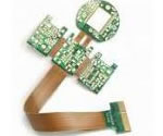
Flex PCB overlay film Flex PCB application
China Flex PCB Manufacturing, Shenzhen Flex PCB Manufacturer, Making Flex Circuit boards
Flex PCB Contract manufacturer, PCB Fabrication, Turnkey assembly services
Buy Flexible Print circuit board, customer: /USA/UK/Canada/South Africa...
Flex PCB Supplier Shenzhen, China, Flex PCB Manufacturer, Turnkey services
-
PCBSINO is the Top 5 PCB manufacturer company in China.
PCBSINO do rapid Flexible PCB Prototype within. we can make Flexible Print circuit boards and Rigid circuit boards, Flex and Rigid Flex PCB, single side, double side, multilayer Flexible print circuit board
PCBSINO making many type electronic product for our customer, Our turkey services team can source original components part for your project(Digikey/Mouser/RS...), senior Electronic engineer will follow each step of the production to solve any PCB problem and our team will do final function test in PCB house.
Flex PCB |
|
Rigid FlexPCB Rapid Prototype |
| Flex PCB |
|
prototype of Flex PCB |
| Flex Prototype |
|
Rigid-Flex PCB Rapid Prototype China, |
Turnkey Services |
|
Turnkey Flex PCB Assembly Services, |
| PCB assembly |
|
Print circuit board Manufacturing, Turnkey assembly |
| PCBA Assembly |
|
SMT Assembly, EMS/OEM supplier China |
Flex PCB overlay film Flex PCB application
-
Flex PCB overlay film Flex PCB application
Flex printed circuit boards are the method of choice for making engineering work easier when complex geometries are involved.
Savings on space, weight and cost together with increased reliability of the electrical connections are just some of the benefits provided by flexible printed circuit boards.
Our PCBs in the Flex Pool are exclusively manufactured in Germany
4 Key Advantages of Flex Circuits
1) Reduced size & weight
Compared to standard printed circuit boards (≈0.063” thick), flex circuits provide a dramatic decrease in package size and weight. Flex circuits, typically just 0.004”-0.010” thick, are even thinner and lighter than traditional cable options.
2) Solution to interconnect challenges
Interconnect problems can often be solved by flex circuits, which integrate the interconnects into the part. Thus, flexible circuits eliminate the need for expensive cables and connectors.
3) Reduction in assembly costs
With the interconnections built into the flex circuit, fewer connectors are required, and thus less soldering. The ability to pre-form the flex circuit assembly, along with its inherent flexibility, allows quicker installation, particularly in hard-to-reach areas.
4) High performance & flexibility
Certain applications simply require circuits that can flex. Compared to other flexible options, flex circuits provide superior electrical and mechanical performance.
DuPont Teijin Films manufactures a range of PET polyester films that are ideally suited for use in flexible circuitry applications, whether Flexible Printed Circuits (FPC) or Flat Flexible Cable (FFC).
Printed Circuits for Wearable Electronics
The wearable electronics market represents a broad and diverse offering of commercial products that is forecasted to grow into a multi-billion dollar a year industry. GSI Technologies is at the forefront of manufacturing and leading development efforts on wearable products where printing solves technical issues. GSI utilizes ink sets including Silver (Ag), Silver/Silver Chloride (Ag/AgCl), carbon, and dielectric inks from multiple vendors. These inks sets are specially designed for use with flexible substrates. The flexible substrates have included a variety of TPU (thermoplastic polyurethane) based materials. Along with materials knowledge, GSI is able to use its manufacturing capabilities such as sheet or roll based through hole printing and high precision laser converting to enable new product designs. With our downstream converting partners, wearable parts can also have adhesive applied, be final packaged, and sterilized.
Printed Circuitry Capabilities
GSI’s printed electronics manufacturing expertise is fully capable across most polymer thick film constructions specializing in printed silver flex circuits. Investments and partnerships enable capabilities to produce single, double sided, and multi-layer circuits. Capabilities exist to pre-process film or paper substrates with selective place openings (vias) or surface chemistry prior to creating 100% additive conductive structures. Available capabilities include:
Extremely broad range of materials selection including silver, silver/silver chloride, carbon, graphene, nickel, iron, tungsten, bismuth, zinc, PEDOT, and blends such as platinized carbon. Processing ITO films with IR laser ablation.
Relationships
GSI services numerous customers with our conductive printing capabilities. We have formulated strategic partnerships in North America, Europe, and Asia to satisfy market demands for secondary operations.
Experience
Flex-rigid fabrication is a mature technology, with well developed rules for success. The first is to establish and maintain a dialogue with the board fabricator and to ensure that any modifications to design rules or design checks (DRC) are imported into the layout package in use and adhered to.
Many of the guidelines for a successful outcome of a flex-rigid design flow from the properties of the materials being employed. The base material for the rigid portion is most likely to be FR4, while the flex is typically a polyimide film (often called Kapton, after DuPont’s material) with copper foil applied and a coverlay film imposed in place of the solder mask.
Some thought is needed about how the material properties match the task and this quickly shows where care should be taken. The copper-to-film bond is a junction between dissimilar materials; the tighter the bend radius, the greater the stresses at the boundary and the higher the risk of delamination. The tracks, although thin, are copper and if the bend radius is too small, repeated flexing carries the risk of stress fracture.
The transition between rigid and flex is also an important area; as with cable termination, bending forces should not be imposed at the transition as this can create very small bend radii over a small distance. Again, dynamic modelling of folding in 3D is helpful and the composition of the layer stack-up is key for reliability and manufacturability.
Many common errors can be avoided by attention to a few key points in the design process. One area is the need for a larger copper ring around any hole drilled in the flex and, as a related point, the need to leave a larger separation between drill hole/pad and adjacent tracks. The flexible film is just that and the effect of that flexibility is to increase normal (inescapable) tolerances. Therefore, if a drilled hole misses concentricity with its pad by a small margin, the hole will still plate and connectivity through the via will be unaffected – but there is a risk of a short to a track passing too close.
Minimising vias in the flex region is desirable in itself; the cost of vias is higher than in the rigid, assuming the design requires a double sided flex. This is one area where the configuration of the stack-up that makes up the complete PCB is critical. The manufacturing process is in part subtractive – there will be layers over and under the flex in fabrication that are removed selectively to release the flex segment before the process is complete. The stack-up should be configured to ensure the polyimide layer is fully supported through any drilling. Visualising a drill bit attempting to penetrate a thin, deformable film will immediately show why.
Transition
Merely taking vias in the flexible area back into the rigid portion – the flex layer runs throughout the total area of the PCB and provides flexibility only where it is exposed – is not sufficient. For manufacturing reasons, the transition from flex to rigid is not at the same point throughout all layers, so any (possibly buried) vias in the flex layer must step back into the rigid area by a larger margin than might be obvious. Where tracks join circular pads in the copper of the flex layer, teardrops should always be applied; the gradual transition from linear to circular eliminates a possible stress point at the junction.
Use of copper on the flexible layer or layers also adds to the list of ‘special rules’ and visualising what is happening when the flexible segment is called into action will show why.
A common error is to have too much copper on the flexible layer – large areas of metal foil bonded to the polyimide will inhibit flexing. If continuous copper is needed, then an appropriate level of cross-hatching will be required. For similar reasons, tracks should be routed perpendicularly to the bend line. All copper should be derived the original foil as plating on the flexible surface tends to produce crystalline metal that is too brittle to guarantee long life.
Apart from the thickness of the polyimide, the materials mainly differ in their adhesive systems (glueless or on epoxy or acrylic basis) as well as in the copper quality. For comparatively static bending applications with a low number of bend cycles (for assembly or maintenance) ED (electro-deposited) material is adequate. For more dynamic, flexible applications RA (rolled annealed) materials must be used.
Materials are selected on the basis of the product and production specific requirements, and the datasheets of the materials used can be requested as required.
Adhesive systems:As a bonding agent between the flexible and the rigid materials, systems using adhesive on an epoxy or acrylic basis (which is still capable of reacting) are used. The options are as follows:
Composite film (polyimide film coated on both sides with adhesive)
Adhesive films (adhesive systems poured onto a paper base and covered with a protective film)
No-flow prepregs (glass mat/epoxy resin prepreg with very low resin flow)
CONTAG mostly uses no-flow prepregs as bonding agents.
3. The characteristics of flexible materials
Flexible materials differ from rigid materials in their essential characteristics, which have to be taken into account:
Significant reduction of copper adhesion at higher temperatures (e.g. when soldering)
Increased water absorption
Changes of dimensions which are larger, by a factor of up to 10 in the individual production stages, especially for wet processes
Single and multi-level thin-film prototyping and production
Metrigraphics partners with component designers like you to envision, prototype, and produce innovative thin-film circuits and components. Having served a wide variety of demanding aerospace, defense, telecommunications, commercial printing, and photonics clients over the last 30 years we’ve honed our skills and offer a wide choice of materials on which we can produce your circuits. We can deliver down to submicron levels with industry-leading circuit densities and with impressive yields. Six or more layers are achievable, including conductive layers that are independently stacked, aligned and interconnected.
To ensure that your design is delivered in the shortest lead time, it is best to supply us with a scaled vector drawing. This should include locations of components and buttons and have a complete BOM of required parts.
With Flexible Circuits, where components are attached or where the flexible circuit board is to be bent as it attached to the device, stiffeners are required.
Why? Stiffeners prevent damage to the copper traces of the Flex PCB and are made to the exact height of the insertion point of the connector.
Flexible PCBs, by their nature can be made to odd or intricate shapes; they may not be a convenient rectangle. After the Flex PCB is manufactured, it has to be cut to shape, a machined metal tool will be required and with most projects off tool samples will be supplied for approval. Small production runs and Prototypes will also need tooling; the same tooling can also be used for larger production runs as your requirement grows.
When there will be continuous or dynamic flexing of the circuit material, special considerations are needed. On multi-layered Flex PCs, this includes taking into account the number of layers while making sure that the conductors will not be fatigued when the FPC is flexed.
Flexible printed circuit from Reid Industrial Graphic Products are designed and fabricated to the highest quality standards using only the best materials.
4. Layout guidelines
From the differences mentioned above, for the layout and use of rigid-flex printed circuits, the following can be deduced:
For single-sided flexible circuits, the bending radius is approximately 6 x the thickness
of the flexible material, and for double-sided circuits it is approx. 12 x the thickness.
Choose track widths and spacing in the flexible region to be as large as possible (> 150 µm)
The flexible region should have parallel tracks which are the same width, with the same leakage resistance, and which run at 90° to the bend line
Tracks should extend at least 1 mm into the rigid region
On flexible layers, include hatched copper areas which are as large as possible
The tracks on double-sided, flexible parts should be symmetrically offset
Holes should be at least 2 mm away from a flexible part
Choose solder surfaces to be as large as possible, the diameter of solder eye pads should be at least twice the diameter of the hole.
Solder must not come closer than 1 mm to the flexible area
Add about 1 mm all round to the dimensions of openings in non photostructured covering films
To be able to assemble the components on a board, to solder & check them, a stiff frame with defined breaking points should be used. Blanks can contain single or multiple boards.
Always use smooth (round) milling transitions to the connected parts of the circuit
A variant on the rigid/flex formula is the application of stiffening to a portion of the flexible layer. In effect, this delineates a region of the assembly that is rigid, but which does not carry components. Stiffeners can provide support during assembly and can constrain the shape of the flexed circuit or they can provide structure and minimum thickness where the flex layer terminates by entering a zero insertion force connector. Although only providing mechanical support, the same set of rules applies to avoid creating problem areas.
Those designing flexible PCBs have often found value in making paper models of their boards – ‘paper dolls’. Today, 3D representation of the design can provide that insight into real world geometry, while applying the parameters the board fabricator requires for high yield. By drawing accurate component profiles from its database, engineers can be certain from the outset that the flexed and folded product will fit together as intended, with no interference.
GSI has an extensive and very broad engineering team with collective experience in excess of 150 years. The GSI team has helped many companies solve difficult technical problems not solved by other manufacturing partners.
Scale
Flat-bed print lines are utilized to support early stage process development and for producing production representative prototypes. As volume grows our roll-to-roll print lines have the print speed and drying capacity to support high volume requirements. In excess of 14 billion sensors have been produced on GSI’s installed manufacturing base.
Quality
All application development and manufacturing is performed within an ISO 9001 and ISO 13485 certified quality system. Automated print lines are outfitted with proven vision inspection and 100% real time electrical testing supported by statistical process control systems ensuring high yields and consistent product quality.
Conductive circuit printing in sheet and roll to roll format
Substrate widths: 500 mm web and 600 mm sheet
Handling of films down to 2 mils in thickness
Experienced with traditional conductive inks and many new technology developments (nanoparticle systems)
Ability to change the design resistance by 9 orders of magnitude through ink selection
Full range of UV and thermal curing systems
Multi-layer flex circuits including thru hole printing (vias)
Laser ablation of transparent conductors
Secondary die cutting by hard tool or laser
Statistical process control
Dedicated engineering team to assist in manufacturing flow optimization
Flex circuit board is customized. Its conductive inks (silver / carton, dielectric and other functional…) are effectively cured through heat, UV and IR radiation and are used for the production of membrane switches, Keyboards for desktop, heating elements, automotive sensors, Touch screens, EL lamps.
Flexible printed circuit board, it can work with multi-sides. The single-side flexible circuits have a single conductor layer made of either a metal or conductive (metal filled) polymer on a flexible dielectric film. The component termination features are approachable only from one side. Holes can be formed in the base film (PI + Copper) to allow component leads to pass through for interconnection, normally by welding. The surface can be covered by protective-coating over circuit or without. Also it can be welded on many components such as led, resistant, Metal-dome and more. on and allowed the board to conform to a desired shape, or to flex during its use.
more flex circuit board catalogues.
Flexible circuits are members of electronic and interconnection family. They consist of a thin insulating polymer & polyester sheet having conductive circuit patterns affixed thereto and typically supplied with a thin polymer coating to protect the conductor circuits.
Flexible PCB is also called flexible circuit, including one metal layer, double sided, multilayer and rigid flex circuits. The circuits can be formed by etching metal foil cladding (normally of copper) from polymer bases, plating metal or printing of conductive inks among other processes. Flexible circuits may or may not have components attached. When components are attached, they are considered by some in the industry to be flexible electronic assemblies.
Suitable uses include:
For use in copper laminates and adhesive overlays
For applications including automobile systems such as dashboards and flat wiring solutions, heating systems, appliances, RFID tags and labels, smart card lead frames and antennae and many others
What Do You Mean “Flexible Printed Circuits Aren’t Printed”?
It’s no wonder that circuit terminology can be so confusing. After all, the most common circuits in the world, printed circuit boards (PCBs), are not, in fact, printed…they’re etched! The same goes for flexible printed circuits (FPCs). To help clear things up, below you will find short descriptions of the most common types of circuits:
Flex Circuit, Flexible Circuit, or FPC: Copper-cladded film (usually polyimide) that is chemically etched to produce a specific circuit pattern.
Printed Circuit or Membrane Switch Circuit: Conductive polymer Ink, usually silver, screen printed on thin film, typically polyester, to create a specific circuit pattern.
Flat Flexible Cable, or FFC: Thin copper conductors that are laminated between two layers of polyester insulators to create a cable.
Printed Circuit Board, or PCB: Copper-cladded, fiberglass-reinforced (rigid) laminate that is chemically etched to produce a specific circuit pattern.
PRICE CALCULATION
The minimum surface area for calculating the base price is 1 dm².
A surface area of up to 5 dm² is possible in the Flex Pool.
We offer delivery times of 10, 16 or 22 business days.
Please feel free to have larger unit quantities calculated using PCB-OVERSEAS.
For furhter information, please feel free to contact us, www.pcbsino.com