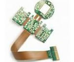
Portable wireless electronic device Flex PCB application
China Flex PCB Manufacturing, Shenzhen Flex PCB Manufacturer, Making Flex Circuit boards
Flex PCB Contract manufacturer, PCB Fabrication, Turnkey assembly services
Buy Flexible Print circuit board, customer: /USA/UK/Canada/South Africa...
Flex PCB Supplier Shenzhen, China, Flex PCB Manufacturer, Turnkey services
-
PCBSINO is the Top 5 PCB manufacturer company in China.
PCBSINO do rapid Flexible PCB Prototype within. we can make Flexible Print circuit boards and Rigid circuit boards, Flex and Rigid Flex PCB, single side, double side, multilayer Flexible print circuit board
PCBSINO making many type electronic product for our customer, Our turkey services team can source original components part for your project(Digikey/Mouser/RS...), senior Electronic engineer will follow each step of the production to solve any PCB problem and our team will do final function test in PCB house.
Flex PCB |
|
Rigid FlexPCB Rapid Prototype |
| Flex PCB |
|
prototype of Flex PCB |
| Flex Prototype |
|
Rigid-Flex PCB Rapid Prototype China, |
Turnkey Services |
|
Turnkey Flex PCB Assembly Services, |
| PCB assembly |
|
Print circuit board Manufacturing, Turnkey assembly |
| PCBA Assembly |
|
SMT Assembly, EMS/OEM supplier China |
Portable wireless electronic device Flex PCB application
-
Portable wireless electronic device Flex PCB application
Brain-computer interfaces (BCI) for medical and non-medical applications has made substantial progress in last few decades, and has been applied in various areas, such as control of motion and electrical stimulation treatment of paralyzed persons etc.1. For medical and clinic applications, such as identification of epileptic foci for clinical purpose, devices with microelectrodes to record electrocorticogram (ECoG) signals are necessary. An array of microelectrodes placed directly on the cortical surface of a brain could record spatial distribution of neural activity with high accuracy2, and provide detailed information of cognitive behavior of a brain. Therefore an array of microelectrodes could serve not only as basis for weakly-invasive high-performance BCIs, but also as ECoG electrodes which have broad medical applications. For instance, it could be used to stimulate the areas of a brain to assess the risk of eloquent cortex damage during a surgical resection, as the control auxiliary devices to help patients to move their injured limbs, as a meditation for drug addicted person etc. The ECoG electrodes array are particularly useful for those with motor disabilities who need a communication device to guide the mobility, and those paralyzed who use ECoG to control their muscle etc.3. For epilepsy patients, it is important to know when they are under attack. Therefore, a portable wireless ECoG system is convenient for doctors to monitor patients’ conditions.
By using a set of high-speed printing methods, printed electronics solutions can deliver exceptional performance in many applications at a significantly lower cost. For example, Molex® uses conductive ink (typically silver or carbon) that is selectively deposited only where needed onto a PET substrate via sheet fed screen-printing or a roll-to-roll process. Then the ink is cured thermally or via ultraviolet light. Multiple print and cure passes are made if multiple signal layers are required. The additive printing process is highly efficient, produces little waste and does not require the use or disposal of chemical etchants.
While the PET substrate provides temperature stability, high-temperature processing or curing can be problematic when working with a PET substrate and can lead to shortened component life or damage to an assembly. Molex proprietary component attachment processes allow a lower temperature profile. LED lights and other standard surface mount components are bonded to the silver circuits using traditional pick-and-place and reflow equipment. An additional step dispenses an encapsulant over the bonded components to enhance mechanical rigidity. The conductive silver traces are adequate to cool low-power backlit LED packages, thereby eliminating the need for heat sinks and design tricks like thermal vias or complicated thermal pathways.
Advancements in silver ink screen-printing allow printed traces as narrow as 0.127 mm with spacing as small as 0.127 mm on PET. The development of low resistance inks makes a particularly effective circuit for a wide variety of low-power and low-signal applications. Advancements in bonding have been developed to overcome restrictions on attaching fine-pitch microprocessor-based components on PET via traditional surface-mount technology (SMT) processes that apply low-temperature solder paste to screen printed silver ink pads. This new proprietary process developed at Molex allows the attachment of right-angle LED backlighting for enhanced user-interface applications, in addition to resistors, capacitors, sensors, RFID and other passive devices.
The printed silver circuit manufacturing process yields flexible all-in-one Molex Soligie® printed electronics LED lighting assemblies with a standard commercial component lifespan, at a lower overall cost than conventional circuitry. Depending on the application, screen-printing silver on polyester can save 50 percent or more on substrate costs compared with an equivalent copper circuit.
ECoG microelectrodes normally are a flexible planar structure. The electrodes are small in dimension, providing much higher spatial resolution, better signal-to-noise ratio (SNR) and broader bandwidth compared to electroencephalograms (EEG) systems, and they have more stable measurements compared to micro-needle electrode arrays4. ECoG recording system has been regarded as a promising tool for BCIs-based medical and welfare applications5. However, most of the ECoG system requires wire connections for communication, which is not portable. A wireless ECoG system is therefore desirable and necessary. For long-term, real-time and portable observation and medical intervention of disordered patients, a mobile phone based ECoG system with wireless communication and control capability would be practically useful. This paper reports a wireless ECoG recording system with a flexible and biocompatible electrode device with an array of 32-microelectrodes. Based on a rat’s epilepsy treatment experiment, we show the ECoG system can record brain activity and perform electric stimulation wirelessly, demonstrating its potential for broad applications.
Active thermal monitoring and power management is important to throttle back performance and prevent the device from exceeding the comfort zone. This requires adding thermal sensors on the silicon and in the system to monitor operation and power. The information is used in combination with clock management to make real-time adjustments in operation frequency. Ideally this function would integrate onto the processor, but it also can be combined using flex circuits or in the package to provide active monitoring.
Materials And Environment
The human body is not an ideal environment for electrical components. While the temperature range for worn devices may be limited, the environment itself can be harsh. Electronics are expected to function in very moist and dusty conditions. Fitness band manufacturers learned early on to design for everything from jostling and exposure to sweat in the gym to direct exposure to moisture in the shower. Many materials used in package and board assembly remain sensitive to moisture, requiring full encapsulation of all electronic components. Design has to address concerns for material interaction, reliability of interfaces, and impact on the thermal environment.
Concerns for exposure to certain elements and materials are also important to address. Packages need to not just be green, but also reflect the impact of skin-based sensitivities and standards defined for medical electronics. Meeting lead-free standards increasingly drives use of conformal coatings to reduce sensitivity for tin whisker growth. When a device is operating under strain, something more common in flex circuits, tin whisker growth can be accelerated. Use of conformal coatings on electronics as well as system-level encapsulation increases the number of material interfaces that can delaminate and fail if not properly designed.
Material interaction has both a chemical and a mechanical element driving calibration and testing to optimize the package, the coating, and even the encapsulation used in the end system. Less knowledgeable end customers typically will rely on the component manufacturer to ensure compatibility and to provide calibrated models for both mechanical assessment and reliability. Many of the mechanical-based interactions can be brought out with temperature-based cycling including moisture-based and pressure-based testing. Due to metal migration concerns, biased testing is increasingly important to validate sensitivity in moist environments and to validate the risk of tin whiskers.
Many companies have added requirements for package component bend testing, a direct result of the dominance of thin PCB, thin package, and flex-based circuits in wearables. The impacts of stretch and deformation extend further than the package connection to the PCB. Stress also can affect circuit operation, especially noticeable with MEMS used in sensors.
MEMS sensors rely heavily on components that detect changes in resistance or capacitance for metal and dielectric structures. When these structures deform, the values will change, causing a false signal or throwing off the calibration. Transistors on semiconductor wafers also can be sensitive to these effects as well. Stress causes deformation that changes how the transistor performs. As packages and system interconnects are made thinner, flex-based deformation is a real concern for electrical operation and reliability.
Without a doubt, circuit co-design extends to the package to ensure operation of the device under stress conditions. Analysis of stress on the semiconductor circuitry is highly complex and requires characterization of the package and silicon during development. In some ways the effects can be simplified by limiting the thickness and rigidity of the package and silicon interface.
To truly achieve the form factor requirements of wearables, a more complex circuit model and design is optimal to account for electrical variation and ensure performance. In this way, wearables will continue to blur the lines between circuit, package, and end system.
This just scratches the surface of packaging requirements for wearable electronics. Some products that are meant to integrate with clothing also have to address survivability while being cleaned or washed. Others require new models to represent shock and common wear and tear. Defining what is needed in terms of robust reliability testing for electrical components going into wearable products is certainly a new field in the making.
AlphaEMS provides a variety of flexible PCB assembly solutions for the latest in printed circuit board technologies. We provide the highest level of customer satisfaction and deliver premier quality to our design engineer customers using our high-tech flexible PCB assembly facility located in Fremont, California.
Flexible PCBs are widely used in everyday electronics such as portable electronic devices and small/miniature devices where weight reduction and maximum use of 3D spaces is required. Common applications for flexible PCBs include consumer electronics, medical, industrial, aerospace, military and transportation electronics.
Flexible Printed Circuit Board (PCB) Benefits
Increased system reliability
Flexible PCB assembly error reduction
PCB assembly cost reduction
Decreased assembly time
Reduction of package size and conforming to space constraints
All procedures conformed to the Guide for the Care and Use of Laboratory Animals (China Ministry of Health) and had been approved by Zhejiang University Committee on animal usage. Sprague Dawley rats weighing between 250–350 g were used in our experiments.
Fabrication of flexible microelectrode array
The electrode device has an array of 32 microelectrodes, with a total width of 16.3 mm and length of 24.8 mm made on a PI film. The fabrication process is as follows: A (Polymethyl methacrylate) (PMMA) layer was spun coated on a glass substrate as the sacrificial layer for removal from the glass which was used as a support for easy fabrication, and was baked at 180 °C for 30 min; then a 60 μm PI layer was coated on top and baked at 230 °C for 180 min. After baking, microelectrodes were formed by photolithography and lift-off process. A Cr layer of 20 nm thickness, Ag of 600 nm and Cr of 20 nm were deposited by sputtering in sequence. Both the bottom and top Cr layers were used to improve adhesion of metal with the PI layers. A 600 nm thickness of Ag layer was used to achieve low impedance for better signal acquisition with low noise, yet to have sufficient flexibility. Then, another PI layer about 10 μm was coated on top of the Cr layer for insulation and baked at 230 °C for 180 min. The microelectrode array were patterned and etched by oxygen plasma to open windows of metal layer for electrical contact and holes for drug injection. Au of 60 nm thickness was then electroplated on the windows and holes of the Cr top layer to achieve better contact with neurons and to improve the conductivity of the microelectrodes. Once completed, through acetone steeping, the ECoG electrode with the PI layer was removed from the glass substrate using the PMMA as the sacrificial layer. A flexible printed circuit (FPC) board connector was used to connect the 32 microelectrodes of the ECoG electrode device.
The device consists of a temporary tattoo—which sticks to the skin, induces sweat and electrochemically detects the alcohol level—and a portable flexible electronic circuit board, which is connected to the tattoo by a magnet and can communicate the information to a mobile device via Bluetooth. The work, led by nanoengineering professor Joseph Wang and electrical engineering professor Patrick Mercier, both at UC San Diego, was published recently in the journal ACS Sensors.
“Lots of accidents on the road are caused by drunk driving. This technology provides an accurate, convenient and quick way to monitor alcohol consumption to help prevent people from driving while intoxicated,” Wang said. The device could be integrated with a car’s alcohol ignition interlocks, or friends could use it to check up on each other before handing over the car keys, he added.
This work was supported by the National Institute of Biomedical Imaging and Bioengineering of the National Institutes of Health (grant no. R21EB019698), the Defense Threat Reduction Agency Joint Science and Technology Office for Chemical and Biological Defense (grant no. HDTRA1-16-1-0013) and the UC San Diego Center for Wearable Sensors.
Incredible shrinking medical devices require circuitry within tight space and weight parameters, and fast heat dissipation with increased airflow. Anybody who ever packed a suitcase or organized a cluttered closet knows firsthand that the ability of contents to bend or flex is essential to maximizing space and efficiency. Among a number of proven technologies migrating from consumer electronics into medical devices, flex circuits and flexible printed circuit connectors can help designers optimize space in tightly packaged medical devices.
Occupying three dimensions, flexible printed circuits can be bent around packaging and even folded over to fit in a much smaller device enclosure. There are a number of other distinct advantages. Flexible substrates with single, double-sided, and multi-layered circuitry are ideal for high performance signal and power connections at an economical applied cost. Flex products can also be mounted in through-hole, surface mount and press-fit configurations.
Sensors & Sensing
For companies interested in creating high-value, low-cost sensor applications, PARC can customize, build, and integrate sensing electronics into the desired form factor. Set up for low cost and disposability, PARC's printed and flexible electronic expertise can be applied to consumer health and electronics products, high-functionality packaging, and electro-mechanical sensing in a broad range of medical and biomedical applications.
Micro Assembly Printer. Electronic chips as Ink
PARC is developing a revolutionary new printer system for making electronics and smart materials. Inks for the printer would be composed of millions of small pre-fabricated semiconductor chips. The printer system would output functional high performance electronics systems such as heterogeneous sensor arrays and displays. For more details see project page.
Electronics Design & Prototyping
This suite of services is targeted at clients who require hardened prototypes to demonstrate their materials, fabrication tools, or product ideas. In addition to printed electronic components, these prototypes can include other thin-film electronics elements fabricated by conventional large-area electronics and conventional silicon circuitry from chips to printed circuit boards. PARC provides design and fabrication of "proof-of-concept" level demonstrators and, with its manufacturing partners, can provide a seamless path to volume manufacturing. For more information, please visit our prototyping services page.
Compliant High-Density Interconnect for Semiconductors and Optoelectronics
PARC has invented and developed a compliant high-density interconnect (HDI) technology, based on our ClawConnect platform, that enables ultra-thin, ultra-small, high-performance, high-compliance interconnect solutions with low total cost of ownership and without sacrificing quality and reliability. Applications that can realize multiple benefits include MCPs, MCMs, chip-on-board (COB), chip-on-carrier, wafer-level packaging (WLP), single in-line packaging (SIP), land-grid array (LGA), tab bonding, flexible electronics, hybrid silicon to printed electronics attachment, and interposers and probe cards.
MEMs Technology
PARC has developed a remarkably versatile method for producing 3D micro-structures based on our ClawConnect platform technology. To date, we have demonstrated high Q-factor integrated on-chip inductors for cell phone and other wireless applications, large stroke (up to 100 µm) electrostatic actuators (binary or analog), laser beam steering or scanning mirrors, and more.
Some components are a little more difficult to flex, but fortunately there’s a general trend in electronics that can help. “The trajectory of the traditional semiconductor industry is all around miniaturization—making things smaller and thinner,” John Rogers, a professor in engineering from the University of Illinois, told Gizmodo. “Those trends have relevance and importance for flexible electronics.” That means that some parts—like radio antennae and simple sensors—are naturally starting to become so thin that they’ll be flexible enough without much extra research.
A Flex PCB is an arrangement of patterned circuitry that is printed as well and a number of components that use material that is flexible; there are those that have cover lay and those that do not. These flexible materials are sometimes fabricated by using components that are normally used in ridged circuit boards that are printed. The components are important because they make it possible to acquire a shape that is not only desirable but very flexible. In simple terms, a Flex PCB is a device that is made up of a number of conductors that are bonded to a dielectric film that is thin. These devices where invented to replace the wireless harnesses that were used in the past. There has been amazing exponential growth in the improvement of these devices from the era of World War II to today where so many appliances rely on this device to function as expected.
Better Packaging
Flex circuits are also a potent tool for improving electronic packaging. A well-designed mechanical package that’s consistent, mechanically sound, and promotes airflow may include a wide variety of electronic components, including connectors, transmitters, receivers, resistors, capacitors, etc. Those components must be contained in a tightly packed, electrically interconnected package. Flex circuits make that possible. Unlike rigid circuit boards, which only allow circuit traces in the X and Y plane, flex circuits allow designers to route circuits along curved surfaces and in multiple directions on any axis.
Designing an effective package is a collaborative process involving device designers and their suppliers. Flex circuit designs always contain tradeoffs in electrical and mechanical performances. Molex works with its customers on issues such as optimum routing of flex circuits in packages to optimize signal strength and mechanical integrity.
Those package designs may also include “rigid flex” circuits. These circuits include both rigid and flexible substrates laminated together in a single structure. For example, there may be a section of the device with several electronic components — resistors, capacitors, connectors, processors — that is rigid, but a flexible electrical “tail” leads from the rigid section, eliminating the need for an interface connector.
Flex PCBs are very important electronic devices that are used in very many appliances; both complex and simple systems. Some common appliances that use a flex PCB include: printers, portable devices such as mobile phones and hard disks. These are however not the only flex PCB applications. There are a number of industries that incorporate this device into their inventions. Examples of these industries include: communication, transport, military, aerospace, automotive, medical and electronics industry. The transportation industry specifically benefits from this device since it is able to resist movement and vibrations which is an important feature for this industry.
In order to get a flex PCB that works as it should, different industries rely on companies that have the expertise to create these devices for different applications. The problem with this however is the fact that there are so many people who deal in the creation of flex PCB. For this reason, it can be quite challenging for individuals and industries to find the best person in the business. There is however some companies that have managed to stand out from the rest by providing high quality services. It is easy to identify these companies through simple online research that helps you know about different services offered and the quality of service you can expect from each company. These services are however best sought from companies that have qualified and experienced individuals. It is however highly recommended to have such an expert working for you in case you run a big business which produces a number of gadgets that may require the Flex PCB.
The proliferation of smartphones and wearables has, after all, driven chips to grow ever smaller—just look at Intel’s Curie, which packs a processor, simple sensors and Bluetooth into a button-sized unit. As Rogers sees it, small islands of inflexible components, like those already used in these kinds of devices, could sit on elastic sheets. Connected by elastic conductors, they can be positioned so that the kinds of motion the device is designed to withstand failure. “There used to be a belief that you’d have to develop entirely new classes of semiconductor and materials, and that it was all going to have to be inkjet or screen printed,” he said. “But now the winning strategy will recognize those kind of approaches, but also the extreme power in existing technology that’s been developed for portable electronics with more conventional form factors.”
Another option is to share resources that happen to be nearby: there may be no need for a device to come packed with powerful hardware when a lightning-fast smartphone is around. We’ve seen that with smartwatches to some extent, and there’s no reason it couldn’t be the case for most flexible devices either. All that’s required is some kind of wireless data link to quickly beam information back and forth.
OEMs often approach us to help them develop integrated solution(s) for portable devices across a broad range of industries. Imagine what a design for a military or commercial application would be subject to. It could need to withstand harsh shock and vibration conditions and needs be built so that the device is not easily broken. Each end product we manufacture needs to meet specific requirements depending on where and how the device will be used. As new technologies are developed, revisions are made so the existing products become slimmer, smaller, and lighter.
It is common to see packaging requirements for devices of this nature become an issue. With the decrease in size, the internal electronics need to be redesigned to fit the available space. For example, inside the molded plastic case, there may be a battery pack and a two button user interface. That wouldn't leave much space for multiple circuit boards and a type of interconnecting solution.
Solution
Once the engineering team has reviewed a customer's engineering data and the blueprint, the molded plastic casing process would proceed. Working directly with customer engineers, we are able to provide solutions that best fit for the minimal packaging requirements, like implementing a 6-layer rigid-flex circuit board.
This rigid-flex PCB consisted of 4 high layer count rigid circuit board areas and 3 flexible circuit areas. The application required the flexible regions to be a "Bend Once to Fit" design, so we needed to take into consideration the bend radius for the flex portions once assembled.
There’s still one major fly in the ointment. “Power supplies are a barrier,” Rogers admitted. “You can make most components small enough in lateral dimensions that you can engineer the soft mechanics you ultimately want.” But that’s simply not the case with batteries, where the capacity of a cell is dictated by its volume: make one thin enough to be flexible, and it barely holds any charge. That’s of little use, especially given the rate at which most devices now chew through charge.
Wireless power is likely the best solution. “In that case all you really need to do is to create flexible antennae to receive the power,” Rogers said. There are already houses in Seattle that are part of an experiment to test how practical that approach might be. There, devices seize the oscillating signals in the data streams of wi-fi and turn it into direct current. Currently it powers only small devices, but at this year’s CES we saw Ossia’s wireless system charge an iPhone in mid-air, which will be a commercial reality by the end of 2016.
Molex flex circuits give the designer greater flexibility and make electronic interconnection simpler and more reliable. Unlike hard board containing woven glass fibers that tend to result in signal loss, the materials, such as polyimide, used in flex circuits maintain signal integrity. Polyimide dissipates heat quickly, so flex does not require cooling from both sides. The flex materials closely match thermal expansion rates, which make it more reliable in hot and cold temperature extremes and temperature fluctuations in mobile healthcare applications.
Device miniaturization using flex circuit technology does require adaptations in production for tighter copper flex spacing and trace width. A precise develop-etch-strip process is required to etch circuits without removing too much copper. Incorporating blind and buried vias can help retain flexibility in designs requiring multiple layers on a flex circuit. Product handling requires extra care to prevent damage to circuit traces.
Using the right materials and manufacturing processes, Molex copper flex delivers sturdy circuitry with high speed capability, impedance control and minimal signal loss for a robust finished medical device. Ultra-reliable flex circuits are excellent for small, lightweight designs with complex high density circuitry. Significantly thinner and lighter than traditional circuit board, flex makes any product naturally lighter, which contributes to overall cost savings and, in some cases, improved patient mobility and comfort.
“When you’re out at a party or at a bar, this sensor could send alerts to your phone to let you know how much you’ve been drinking,” said Jayoung Kim, a materials science and engineering PhD student in Wang’s group and one of the paper’s co-first authors.
Blood alcohol concentration is the most accurate indicator of a person’s alcohol level, but measuring it requires pricking a finger. Breathalyzers, which are the most commonly used devices to indirectly estimate blood alcohol concentration, are non-invasive, but they can give false readouts. For example, the alcohol level detected in a person’s breath right after taking a drink would typically appear higher than that person’s actual blood alcohol concentration. A person could also fool a breathalyzer into detecting a lower alcohol level by using mouthwash.
Recent research has shown that blood alcohol concentration can also be estimated by measuring alcohol levels in what’s called insensible sweat—perspiration that happens before it’s perceived as moisture on the skin. But this measurement can be up to two hours behind the actual blood alcohol reading. On the other hand, the alcohol level in sensible sweat—the sweat that’s typically seen—is a better real-time indicator of the blood alcohol concentration, but so far the systems that can measure this are neither portable nor fit for wearing on the body.
Now, UC San Diego researchers have developed an alcohol sensor that’s wearable, portable and could accurately monitor alcohol level in sweat within 15 minutes.
“What’s also innovative about this technology is that the wearer doesn’t need to be exercising or sweating already. The user can put on the patch and within a few minutes get a reading that’s well correlated to his or her blood alcohol concentration. Such a device hasn’t been available until now,” Mercier said.
The layer on top of the copper foil is called the soldermask layer. This layer gives the PCB its green (or, at SparkFun, red) color. It is overlaid onto the copper layer to insulate the copper traces from accidental contact with other metal, solder, or conductive bits. This layer helps the user to solder to the correct places and prevent solder jumpers.
In the example above green solder mask is applied to the majority of the PCB, covering up the small traces but leaving the the silver rings and SMD pads exposed so they can be soldered to.
Soldermask is most commonly green in color but nearly any color is possible. We use red for almost all the SparkFun boards, white for the IOIO board, and purple for the LilyPad boards.
Silkscreen
A new millimeter wave technology patent surfaced in Europe back in late July that was only discovered this morning. Back in May Patently Apple posted a report titled "Apple Seeks License from FCC Covering new Wireless Millimeter Wave Technology Found in a Recent Patent Filing." In June we posted a report titled "Apple Invents Wireless Charging iPhone Case Accessory using Millimeter Wave Technology." And finally in July we posted a follow-up story to our May report titled "The FCC approved Apple's License for Limited Testing of Millimeter Wave Technology Related to 5G Networks." Apple's European patent title that translates to "Electronic device with millimeter-wave Yagi antennas," provides us with the missing ingredient in Apple's patent surfacing in April regarding millimeter wave that described new "Patch Antennas."
Instead of Apple's patent being published in English in Europe, the published patent is in German and doesn't provide us with any mosaics or patent figures to keep it as mysterious or as secretive as possible. Below are a few translated portions of the German patent:
Apple notes that "This generally relates to electronic devices, and more particularly, to electronic devices with wireless communication circuits.
The white silkscreen layer is applied on top of the soldermask layer. The silkscreen adds letters, numbers, and symbols to the PCB that allow for easier assembly and indicators for humans to better understand the board. We often use silkscreen labels to indicate what the function of each pin or LED.
Silkscreen is most commonly white but any ink color can be used. Black, gray, red, and even yellow silkscreen colors are widely available; it is, however, uncommon to see more than one color on a single board.
Development of electronic circuits
Electronic circuits were developed for signal acquisition, processing and wireless communication with cell phone. Lower power consumption BLE was used for wireless communication and powered with a button-type battery. A TI CC2541 BLE chip was used as the microcontroller unit (MCU) to control the function of RHD2132 (Digital Electrophysiology interface chips). Details of the circuit chip can be found from Figure S3 in Supplement. Balun circuit was used to convert differential signals to single-ended signals and for impedance matching. The decoupling capacitors were applied to filter spikes in signals, and the shunt capacitors to filter high-frequeData and materials availabilityncy noises. A 32 MHz crystal oscillator was used for normal operation, while the 32 kHz crystal oscillator for sleep mode; An Invert-F antenna with a central frequency of 2.4 GHz and 50 Ω impedance was designed for wireless communication. The designed wireless transmission distance is 10 m for this work, and can be easily upgraded according to applications.
For furhter information, please feel free to contact us, www.pcbsino.com