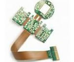
Chip connector Flex PCB application
China Flex PCB Manufacturing, Shenzhen Flex PCB Manufacturer, Making Flex Circuit boards
Flex PCB Contract manufacturer, PCB Fabrication, Turnkey assembly services
Buy Flexible Print circuit board, customer: /USA/UK/Canada/South Africa...
Flex PCB Supplier Shenzhen, China, Flex PCB Manufacturer, Turnkey services
-
PCBSINO is the Top 5 PCB manufacturer company in China.
PCBSINO do rapid Flexible PCB Prototype within. we can make Flexible Print circuit boards and Rigid circuit boards, Flex and Rigid Flex PCB, single side, double side, multilayer Flexible print circuit board
PCBSINO making many type electronic product for our customer, Our turkey services team can source original components part for your project(Digikey/Mouser/RS...), senior Electronic engineer will follow each step of the production to solve any PCB problem and our team will do final function test in PCB house.
Flex PCB |
|
Rigid FlexPCB Rapid Prototype |
| Flex PCB |
|
prototype of Flex PCB |
| Flex Prototype |
|
Rigid-Flex PCB Rapid Prototype China, |
Turnkey Services |
|
Turnkey Flex PCB Assembly Services, |
| PCB assembly |
|
Print circuit board Manufacturing, Turnkey assembly |
| PCBA Assembly |
|
SMT Assembly, EMS/OEM supplier China |
Chip connector Flex PCB application
-
Chip connector Flex PCB application
The general term for COF technology is 'direct chip attachment', or DCA. Aside from the flexible circuit substrates used for COF's, various substrates are available for use in DCA. DCA assemblies are often named based on the substrates used, e.g., chip-on-glass (COG) for glass ceramic substrates, chip-on-board (COB) for printed circuit boards, chip-on-flex (COF) for flex substrates, etc.
Advantages provided by COF technology include: 1) space savings; 2) reduced weight; 3) lower production cost; 4) thermal durability and higher reliability from better heat distribution; 5) shorter time-to-market; and of course, 6) geometrical and mechanical flexibility.
As the result of a unique adhesion soldering process, Würth Elektronik is able to put flip chips on different circuit board substrates – even on flexible materials.
Time and again, a major challenge lies in attaching integrated circuits (ICs) to highly integrated circuit board substrates in a space-saving manner. Würth Elektronik took this challenge on and found an ideal solution with the ESC (encapsulated solder connection) process. The chips are soldered and at the same time glued 'face-down" in their exact position. The ESC process is suitable for the most diverse substrates, be they fragile glass materials, FR4 or even flexible materials such as polyimide foils or LCP (liquid crystal polymer).
Each substrate represents a separate challenge. Depending on the substrate, extremely tiny pitch distances of less than 100 µm can be realized. Using thermal compression bonding technology, the upside-down chip (flip chip) is set onto an anisotropic adhesive containing microscopic soldering particles.
Three basic interconnect schemes are currently in vogue. Each scheme has significant material issues, and all require precise placement and handling.
With controlled collapse chip connection (C4), pad spacing is limited to 0.01-in. or 0.012-in. centers, with the pads typically in an array format. The 95-percent lead/5-percent tin solder bumps do not melt during the attachment process. Solder paste screened or stencil printed onto the flex substrate wets to the bump during reflow, which occurs at 308°C. Upon reflow, the solder bumps on the flip chip and the land pads on the substrate self-align, allowing some degree of misalignment during placement. A drawback to C4 is the limitation of solder printing preventing the attachment of integrated circuits (ICs) with pads on 0.004-in. to 0.008-in. centers.
If the polymer flip chip attach method is used, the contacts may be closer because the epoxy can be stencil printed to finer pitches. For example, epoxy bumps of 0.002-in. diameter have been produced on 0.007-in. centers and on 0.004-in. centers under ideal conditions. However, achieving finer pitches involves a tradeoff because epoxy does not metallurgically wet to the chip's pads or the substrate's lands. As a result, no self-alignment occurs during the reflow process; therefore, placement must be exact.
(c) After tacking into place, remove the tape from the accelerometer and solder the rest of the pads (and perhaps retouching the original tacked solder joints).
Soldering these small contacts can be a bit difficult, but a little practice will make you a pro. There are two main techniques I've used with some success. Both use a standard soldering iron and either standard small diameter rosin-core solder or solder paste (mixture of minute spherical solder particles, activators, solvent, and a gelling or suspension agent). Here I'll cover a method that works with standard solder (see notes at the end of this step or step 2) for solder paste method).
Product offering includes Type I through Type V flex circuits (single-sided, double-sided, multi-layer and rigid-flex) as well as sculptured power flex and bus bars. Our state of the art manufacturing facility builds product to IPC-6013 (Class I, II & III) standards and is ISO 9001:2001 and ISO 14001 certified. Our services include applications assistance; full in-house design, manufacture, assembly, and test of custom flex circuits and flex circuit assemblies. Additionally, we offer a broad collection of controlled impedance flex circuit assemblies.
Amphenol applications support initial flex design through customized hardware design, for total system solutions. The connectors used for flex termination include a two-piece InterCon50™ and InterCon1mm™ connector, as well as C-Byte™ compression connectors and cStack™ stacking connectors.
Summary of design: Surface-mount low-profile male headers for x-OSC connection with the following pins broken out:
– GND and VCC (3.3V)
– 10 input pins broken out to snap pads (with pull-up resistors)
– 6 input pins broken out to pads for additional sensors (with pull-up resistors)
– 3 output pins broken out to RGB led (with resistors)
– 2 output pins broken out to left and right vibration motor
– 11 output pins left unconnected
USB micro plug connected to power x-OSC (USB mini location conflicted with JST from x-OSC).
Two additional small flex PCBs for vibration motors.
Piezo-Resistive Sensing (PRS) probes from SCL-Sensor.Tech are silicon cantilevers with an integrated piezo-resistor. They are used for self-sensing scanning probe microscopy applications. PRSA probes are additionally equipped with a thermal actuator for self-actuating operation. The piezo-resistors are integrated into a matched Wheatstone bridge to optimize the sensitivity and to compensate environmental thermal drift. By using the self-sensing readout no laser adjustment is necessary in comparison to conventional optical readout AFM systems. This gains time during a cantilever change. Furthermore free space above the cantilever opens a door for new applications and various instrument combinations. The cantilever provides a sharp tip for accurate measurements in various applications. The cantilever chip is bonded onto a small printed circuit board (PCB) with a small connector. The loading process of a fragile cantilever equipped with a connector is more easy and save. The counterpart PCB of the cantilever PCB is connected to a low-noise amplifier by a flat-flex-cable.
Populated boards:
Unpopulated boards bottom (left) and top (right) views:
Copper layers (top=red, bottom=blue):
Connections (green=inputs, brown=outputs):
Soldering using rosin-core solder and soldering iron
In this method, a flux pen is your friend. Kester sells "no clean flux" pens (951 Flux-Pen) that can be purchased at any electronics store for about $5. The flux cleans and etches the surface oxides, prevents oxidation of the copper when it is heated, and helps the solder flow when heated by lowering the surface tension of the molten solder so that it spreads and penetrates more readily.
Start off by dabbing the contacts with flux
Tin the tip of the solder iron and clean the tip of the solder iron on a wet sponge
Put a dot of solder on the tip of the solder iron
Tin one of the copper solder pads
Clean the tip of the solder iron again on a wet sponge
Put another dot of solder on the tip of the soldering iron
Quickly touch the solder iron to the tinned copper pad and sweep the tip of the iron up onto the accelerometer lead
In all honesty, the above technique is pretty tough to master and would receive much criticism from my EE colleagues, so I strongly recommend getting some solder paste and a small tipped syringe with which to dispense it.
Keypad "Click" Domes:
One of the leaders of "keypad domes" is a company by the name of SnapTron.com.
One of their pre-made designs has a hole in the middle of the dome to allow an LED to light up through the button! This gives the designer some very very cool visual effects possible.
There's no secret to making flex keyboards. It's a very simple process allowing you to let your creativity flow for very uniquely shaped keypads, never having to accept boring pre-made keypads ever again. All you're basically doing is spray gluing a few layers together and you have a flush, surface enclosure mounted keypad with the tail tucked under the keypad and into the enclosure. Also to reduce the number of "X" & "Y" contact points, we generally want to use one of the common keyboard encoder chips, like the 74C922 to easily handle up to 16 keys with a BCD output for minimal microprocessor pin usage.
You can do the typical "fold over" as we've shown above or make the keyboard a single layered sandwich to include "domes" to give the user a positive tactile "click" when pressed.
With just a little "Googling around" you'll quickly learn the "ins 'n outs" of making your own personally shaped keypad with custom full color fronts using any color laser printer or copier.
Rock on custom keyboard fans and show us what you've made! Make something really cool looking and shoot us some pics. Every subject is worth $20 in free supplies and we even pay shipping.
A solder bump and reflow attachment process recently developed circumvents the drawbacks to the above two methods. This process negates the need for stencil printing and provides the wetting/reflow action that results in the bumps and pads self - aligning. This new method can flip chip attach IC's to perimeter pads as small as 0.002-in. diameter on centerlines down to 0.004 on.
This approach uses plated 60-percent tin/40-percent lead eutectic solder bumps on the IC and gold-plated lands on the flex. The gold-plated lands are compatible with polymer flip chip where silver-filled epoxy is stencil printed onto the gold land areas.
Regardless of approach, temporary or permanent stiffening must be employed to ensure that the flex remains flat during attachment and reflow; otherwise, yields will be low. After reflow and curing of the underfill epoxy, the flip chip site is very robust, and the stiffening may be discarded.
Pick and Place
Proper selection of pick-and-place equipment is key to developing an FCOF assembly process and achieving targeted yields in production. The pick-and-place system should offer high placement accuracy; versatility in independently controlling key parameters such as time, temperature and pressure over wide ranges; and easy repeatability or modification through stored program control.
Flexible substrates are used in 3D connection and mechatronic concepts for reducing the number of connectors needed. They can stand high dynamic bending and are capable of high speed interconnections between different circuit layers. In portable applications, maximum miniaturization can be achieved by folding the PCB.
Typical applications are found in medical devices (hearing aids, insulin pumps, neurostimulator implants), consumer electronics (mobile phones, portable computers, cameras, TFT displays) or automotive systems (sensor modules, engine control units).
Chip (or Die) on Flex rework is essentially a material handling issue – the flex! Thermal profiles reflect the lower substrate thermal mass as compared to a PCB - typically shorter duration and lower air temperatures to reach liquidus.
Support of the flex circuit necessitates alternate vacuum clamping systems and the use of conductive, rather than convective, lower heating.
Briefly heating the adhesive causes the solder particles to melt and results in a true soldering connection between the chip's contacts and the substrate, which creates the electrical contact. The simultaneous hardening of the epoxy adhesive also sets the flip chip firmly into place. The entire process is called flip chip bonding.
“An additional 'underfill process' is not required. In particular, the high exactness of placement and the finely dosed bonding force make it possible to process even extremely brittle substrates without any problems," explains Roland Schönholz, who is responsible for bonding technologies and Lasercavity at Würth Elektronik in Schopfheim, Germany.
The benefit of this kind of construction is low cost — there is no connector involved at all, just the flex soldered directly down to the PCB. The drawback is that the machine used in the LCD manufacturing process to connect them is expensive, and they are near impossible to re-work.
PentaLogix understands that customers are often looking for a one stop shop to handle their flex circuit design, fabrication, as well as assembly needs to reduce product handling and lead time associated with out-sourcing each of these tasks. Whether your idea is a sketch or diagram, we'll help you design a cost-effective interconnect solution. We are also set up to handle component assembly including connectors and various surface mount components. Presented are common capabilities. Come speak to us concerning tighter tolerances or special process requirements.
The connector is a TAB mated to a COF (Chip On Flex) style flex tail or a COG (Chip On Glass) LCD module construction.
This style of connector is designed to be soldered directly to corresponding pads on your PCB by using a hot-bar soldering machine.
Hot Bar Soldering
High volume contract manufacturers will be familiar with this type of construction and its assembly methods.
There are bondmaster machines made by APE that are designed for prototype, rework or repair work. We have had good experience with the APE Bondmaster, and their price is very reasonable ($US4K at last check).
Because of its high bending strength, COF is very useful in device assembly processes that require bending or folding steps. It is also used in assemblies that require repeated movements such as printers.
The substrate material used for a flex circuit depends on the actual application. Substrates used in COF include flexible reinforced boards, rigid flexible boards, and semi-flexible boards.
As in most DCA technologies, COF assembly has only 3 main steps: 1) die attach, or the accurate attachment of the chip to the flexible substrate; 2) wire bonding, or the electrical connection of the chip to the flex circuit using very fine bonding wires; and 3) encapsulation of the chip and wires with a special compound to protect them from the environment.
The chip is attached to the flex substrate using adhesives that can either be conducting or insulating, depending on the device requirement. Aside from providing mechanical stability and electrical conduction (or insulation) to the chip, these die attach adhesives also provide thermal paths by which the heat generated by the device during operation can be released more efficiently.
For furhter information, please feel free to contact us, www.pcbsino.com