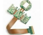
gyroscope Flex PCB application
China Flex PCB Manufacturing, Shenzhen Flex PCB Manufacturer, Making Flex Circuit boards
Flex PCB Contract manufacturer, PCB Fabrication, Turnkey assembly services
Buy Flexible Print circuit board, customer: /USA/UK/Canada/South Africa...
Flex PCB Supplier Shenzhen, China, Flex PCB Manufacturer, Turnkey services
-
PCBSINO is the Top 5 PCB manufacturer company in China.
PCBSINO do rapid Flexible PCB Prototype within. we can make Flexible Print circuit boards and Rigid circuit boards, Flex and Rigid Flex PCB, single side, double side, multilayer Flexible print circuit board
PCBSINO making many type electronic product for our customer, Our turkey services team can source original components part for your project(Digikey/Mouser/RS...), senior Electronic engineer will follow each step of the production to solve any PCB problem and our team will do final function test in PCB house.
Flex PCB |
|
Rigid FlexPCB Rapid Prototype |
| Flex PCB |
|
prototype of Flex PCB |
| Flex Prototype |
|
Rigid-Flex PCB Rapid Prototype China, |
Turnkey Services |
|
Turnkey Flex PCB Assembly Services, |
| PCB assembly |
|
Print circuit board Manufacturing, Turnkey assembly |
| PCBA Assembly |
|
SMT Assembly, EMS/OEM supplier China |
gyroscope Flex PCB application
-
gyroscope Flex PCB application
Introduction to MEMS gyroscopes
(November 15, 2010) — Jay Esfandyari, Roberto De Nuccio, Gang Xu, STMicroelectronics, introduce how MEMS gyroscopes work and their applications, the main parameters of a MEMS gyroscope with analog or digital outputs, practical MEMS gyroscope calibration techniques, and how to test the MEMS gyroscope performance in terms of angular displacement.
The significant size reduction of multi-axis MEMS gyroscope structures and their integration with digital interface into a single package of a few square millimeters of area at an affordable cost have accelerated the penetration of MEMS gyroscopes into hand-held devices.
MEMS gyroscopes have enabled exciting applications in portable devices including optical image stabilization for camera performance improvement, user interface for additional features and ease of use, and gaming for more exciting entertainment. Further applications such as dead reckoning and GPS assistance that require high sensitivity, low noise, and low drift over temperature and time are on the horizon.
Here, we discuss the methods and techniques of quickly getting meaningful information from a MEMS gyroscope in terms of angular velocity and angular displacement measurements.
Accelerometer, Gyro and IMU Buying Guide
Accelerometers and gyros are becoming increasingly popular in consumer electronics, so maybe it’s time you added them to your project! Scrolling through SparkFun’s sensors category reveals a huge list of these sensors that might be perfect for your next project, if only you knew what they did, and which one best fit your project. The goal of this buying guide is to get you speaking the same language as these sensors' datasheets and to help you select the one that is best-suited for your needs.
Accelerometers
What’s an accelerometer measure? Well, acceleration. You know…how fast something is speeding up or slowing down. You’ll see acceleration displayed either in units of meters per second squared (m/s2), or G-force (g), which is about 9.8m/s2 (the exact value depends on your elevation and the mass of the planet you’re on).
Accelerometers are used to sense both static (e.g. gravity) and dynamic (e.g. sudden starts/stops) acceleration. One of the more widely used applications for accelerometers is tilt-sensing. Because they are affected by the acceleration of gravity, an accelerometer can tell you how it’s oriented with respect to the Earth’s surface. For example, Apple’s iPhone has an accelerometer, which lets it know whether it’s being held in portrait or landscape mode. An accelerometer can also be used to sense motion. For instance, an accelerometer in Nintendo’s WiiMote can be used to sense emulated forehands and backhands of a tennis racket, or rolls of a bowling ball. Finally, an accelerometer can also be used to sense if a device is in a state of free fall. This feature is implemented in several hard drives: if a drop is sensed, the hard drive is quickly switched off to protect against data loss.
Now that you know what they do, let’s consider what characteristics you should be looking for when selecting your accelerometer:
Range - The upper and lower limits of what the accelerometer can measure is also known as its range. In most cases, a smaller full-scale range means a more sensitive output; so you can get a more precise reading out of an accelerometer with a low full-scale range.
You want to select a sensing range that will best fit your project, if your project will only be subjected to accelerations between +2g and -2g, a ±250g-ranged accelerometer won’t give you much, if any, precision.
We have a good assortment of accelerometers, with maximum ranges stretching from ±1g to ±250g. Most of our accelerometers are set to a hard maximum/minimum range, however some of the fancier accelerometers feature selectable ranges.
Interface - This is another one of the more important specifications. Accelerometers will have either an analog, pulse-width modulated (PWM), or digital interface.
Accelerometers with an analog output will produce a voltage that is directly proportional to the sensed acceleration. At 0g, the analog output will usually reside at about the middle of the supplied voltage (e.g. 1.65V for a 3.3V sensor). Generally this interface is the easiest to work with, as analog-to-digital converters (ADCs) are implemented in most microcontrollers.
Description: This is a breakout board for InvenSense’s ITG-3200, a groundbreaking triple-axis, digital output MEMS gyroscope. The ITG-3200 features three 16-bit analog-to-digital converters (ADCs) for digitizing the gyro outputs, a user-selectable internal low-pass filter bandwidth, and a Fast-Mode I2C (400kHz) interface. Additional features include an embedded temperature sensor and a 2% accurate internal oscillator.
A combination of ^ 16-g 3D digital accelerometer (Analog DevicesADXL345) and ^ 2000 8 ·s 2 1 3D gyroscope (Invensense ITG 3200) components were located on two sensor islands connected by a flexible printed circuit board (PCB) carrying the power and I 2 C data bus. Chip addresses were arranged so that each sensor island could use an independent I 2 C bus or both islands could share a common I 2 C bus. Twelve data channels were logged at 200 Hz with 12 bits per sample. This gave a greater resolution than previous data collection. The connection between the two sensor islands used two separate flex-PCB strips with two conductors each, as a single strip with four conductors had insufficient flexibility ( Figure 2(b)). The measurement range of the accelerometers aligned with the long axis of the arm was not expected to be sufficient for the fast bowlers and a sufficiently small, high-range sensor was not available.
Product Description
The Pmod GYRO is a 3-axis gyroscope powered by the STMicroelectronics L3G4200D. By communicating with the chip through SPI or I2C, users may configure the module to report angular momentum at a resolution of up to 2000 dps at an output rate up to 800Hz.
Support Materials
Datasheet
Schematics (PDF)
For all other material:
Resource Center
Features:
3-axis MEMS digital gyroscope with high shock survivability
Get angular velocity data with user selectable resolution (250/500/2000dps)
Two customizable interrupt pins
User configurable signal filtering
Power-down and Sleep modes
Small PCB size for flexible designs 1.0 in × 0.8 in (2.5 cm × 2.0 cm)
12-pin Pmod connector with SPI interface and additional I²C interface
Library and example code available in resource center
Using an examplary delivery measured at the wrist, with 650 m·s 2 2 centripetal acceleration at an angular velocity of 2000 8 ·s 2 1 , the radius of rotation was calculated at approximately 0.53 m. At a point on the elbow 20 – 25 cm closer to the centre of rotation, the expected acceleration would be in the range 340 – 400 m·s 2 2 , therefore exceeding the current accelerometer range. This will be remedied in the next sensor development with one manufacturer recently announcing the development of similar-sized 100-g 3D accelerometers. Sensors were attached on the outside of the elbow initially with double-sided tape and then covered over with adhesive bandage. To allow the elbow to flex and straighten, the sensors were attached with the elbow fully flexed, and then the flex-PCB slightly bent to ensure it bowed out when the arm was straight. Accelerometers were calibrated using the six-point method of Lai, James, Hayes, and Harvey (2004) and the gyroscopes were calibrated using integration of a known angle of rotation (3600 8 ).
How do I measure noise density in a gyroscope?
A:
Noise Density provides a useful metric for understanding the trade-off between the total noise and bandwidth of a gyroscope. There are a number of techniques for measuring this parameter, but this example uses the EVAL-ADIS for data collection and a common signal processing technique: the Fast Fourier Transform. The following steps provide an example for producing a Rate Noise Density plot for the gyroscopes in the ADIS16334, a fully-calibrated, six-degree of freedom IMU.
STEP 1: ADIS16334 Installation on the EVAL-ADIS
Connect the ADIS16334/PCBZ to the EVAL-ADIS. Note that this attachment process only requires the ADIS16334BMLZ and flexible connector (green PCB not required in this case). Note that the ADIS16334BMLZ and flexible connector only have 20 pins, while the mating connector, J4, on the EVAL-ADIS, has 24 pins. Make sure that the flexible connector mates to pins 1-20 on the EVAL-ADIS and properly seats into the mating connector on the ADIS16334BMLZ.
Mitigation of block bending in a ring laser gyroscope caused by thermal expansion or compression of a circuit board.
EP 2575415 A2
ABSTRACT
An apparatus includes a sheet of circuit board material, at least one electrically conductive trace positioned on the sheet of circuit board material, and at least one electrically conductive contact pad positioned on the sheet of circuit board material and coupled to the at least one electrically conductive trace. The apparatus further includes at least one deformation point configured to absorb stresses developed in the sheet of circuit board material when the sheet of circuit board material experiences resistance to expansion or compression caused by connection to an object resisting expansion or compression.
IMAGES(9)
Next page
CLAIMS(10)
An apparatus comprising:
a sheet of circuit board material (100);
at least one electrically conductive trace (104) positioned on the sheet of circuit board material (100);
at least one electrically conductive contact pad (106) positioned on the sheet of circuit board material (100) and coupled to the at least one electrically conductive trace (104); and
at least one deformation point (103) configured to absorb stresses developed in the sheet of circuit board material (100) when the sheet of circuit board material experiences resistance to expansion or compression caused by connection to an object (202, 302) resisting expansion or compression.
The apparatus of claim 1, wherein the sheet of circuit board material (100) is created using at least one of flexible printed circuit board, rigid printed circuit board, and a combination of flexible printed circuit board and rigid printed circuit board.
The apparatus of claim 1, wherein the at least one deformation point (103) is created by removing circuit board material from the sheet of circuit board material to reduce a cross-sectional area of the sheet of circuit board material at a first location on the sheet circuit board material.
The apparatus of claim 3, wherein the removed circuit board material (130, 132, 134, 136) has a circular shape.
The apparatus of claim 1, wherein the circuit board material includes a plurality of cutouts (116, 118, 128, 130, 132, 134, 136, 142, 144, 146, 148, 150), each configured to create at least one deformation point in at least one location between a first section and a second section of the sheet of circuit board material, wherein each deformation point absorbs stresses developed between the first section and the second section of the sheet of circuit board material.
The apparatus of claim 5, wherein the plurality of cutouts (116, 118, 128, 130, 132, 134, 136, 142, 144, 146, 148, 150) are arranged on the surface of the sheet of circuit board material in a symmetric pattern.
The apparatus of claim 1, further comprising:
a substrate (202, 302) with a top surface, wherein the object (202, 302) resisting expansion or compression is the substrate (202, 302);
adhesive material (304) attaching the top surface of the substrate with a bottom surface of the sheet of circuit board material (102); and
wherein the adhesive material (304) inhibits the transfer of stresses generated in the sheet of circuit board material (102) when the sheet of circuit board material expands or contracts at a different rate from the substrate (202, 302) to which the sheet of circuit board material is attached.
The apparatus of claim 1, wherein the adhesive material (304) has consistent stress transfer properties across an operating temperature range.
A method comprising:
fabricating a sheet of circuit board material (102) with at least one deformation point (103) between a first section and a second section of the sheet of circuit board material (402);
fabricating at least one electrically conductive trace (104) on the sheet of circuit board material (102) (404);
fabricating at least one electrically conductive contact pad (106) positioned on the sheet of circuit board material (102) and coupled to the at least one electrically conductive trace (104) (406); and
wherein the at least one deformation point (103) absorbs stresses developed in the sheet of circuit board material (102) when the sheet of circuit board material experiences resistance to expansion or compression caused by connection to an object (202, 302) resisting expansion or compression (408).
The method of claim 9, further comprising:
mounting a bottom surface of the sheet of circuit board material (102) to a top surface of a substrate (202, 302) using an adhesive (304); and
wherein the adhesive material (304) is configured to inhibit the transfer of stresses generated in the sheet of circuit board material (102) when the sheet of circuit board material (102) expands or contracts at the different rate than the object (202, 302).
DESCRIPTION
BACKGROUND
[0001]
Ring Laser Gyroscopes (RLGs) can experience performance errors and power loss due to mechanical bending of the laser block. Mechanical bending of the block can occur during exposures to temperature extremes if components are rigidly mounted to the laser block and possess different coefficients of thermal expansion from the laser block material. Laser block bending changes the internal alignment of the mirrors and causes changes in gyro power and performance.
SUMMARY
At the moment I used an Arduino Uno starting kit to start to configure my Android and iOS SDK just to make some proof of concepts.
Right now I am in the phase of choosing the first development board for my physical prototype. The idea is to work on ARM Cortex A for low energy comsumption but also ARM Cortex M is interesting even if I believe that its power will blow away the battery in few days.
Before desigining any custom PCB I want to test out an ARM Cortex, plug my sensors, write the internal OS of the wearable and more forward from there.
Often times, engineers get inspiration from Mother Nature; Velcro, the electrical grid and the Shinkansen Bullet Train are just some examples of inventors taking a cue from what's around them. But that’s not the case with the gyroscope, a device used to measure orientation.
Up until recently the closest thing that resembled gyroscopes were sensors called halteres, club-looking structures that are found in insects such as flies. Halteres help insects navigate and perform aerial acrobatics by offering them important details during flight.
A natural gyroscope
It’s no secret that insects are quite skilled at moving with impeccable precision. In fact, a number of them fly more accurately than our most advanced engineered aircraft. Researchers at the University of Washington discovered that an insect’s wings might also function as a gyroscope of sorts. This new discovery could offer aerospace engineers more insights into natural flight.
The study, titled “A New Twist on Gyroscopic Sensing: Body Rotations Lead to Torsion in Flapping, Flexing Insect Wings,” was recently published in the Journal of the Royal Society Interface. The study’s goal was to find out if an insect’s wings are capable of sensing their body’s rotations during flight. Understanding this would give insight into how insects are able to move rapidly with impeccable accuracy.
What development kit do you suggest me to start with the evaluation of the ARM Cortex MicroCrontroller and mbed OS system?
I have few requirements to start with:
ARM Cortex Micro Controller
BLE Bluetooth
OLED display (touch or non touch)
Memory to save information
LiPo battery
Possibility to test sensors (gyro, vibrations, hearth pulse)
About the sensors I don't really need a development board with already a gyro or other sensors in it. But I want the possibility of tests my own sensors with mbed OS.
It would be nice if you can point me to some development board kits like the Arduino Uno. Then from there my plan is to slowly design various versions of my custom PCB as soon as I have a stable prototype done with the development board.
An apparatus includes a sheet of circuit board material, at least one electrically conductive trace positioned on the sheet of circuit board material, and at least one electrically conductive contact pad positioned on the sheet of circuit board material and coupled to the at least one electrically conductive trace. The apparatus further includes at least one deformation point configured to absorb stresses developed in the sheet of circuit board material when the sheet of circuit board material experiences resistance to expansion or compression caused by connection to an object resisting expansion or compression.
DRAWINGS
[0003]
Understanding that the drawings depict only exemplary embodiments and are not therefore to be considered limiting in scope, the exemplary embodiments will be described with additional specificity and detail through the use of the accompanying drawings, in which:
[0004]
Figures 1A-1C are top view diagrams depicting exemplary embodiments of a circuit board having deformation points to mitigate block bending in a laser block.
Figures 2A-2C are top view diagrams depicting exemplary embodiments of a circuit board attached to a ring laser gyroscope (RLG) and having deformation points to mitigate block bending in the laser block of the RLG.
[0006]
Figure 3 is a side view diagram depicting an exemplary embodiment of a circuit board attached to a RLG with a particular adhesive to mitigate block bending in the laser block of the RLG.
[0007]
Figure 4 is a flow chart illustrating an example method for
DO NOT USE THE SILK SCREEN ON THE FLEXIBLE CONNECTOR TO DETERMINE PIN 1. This is a multi-purpose connector and the pin 1 indicators are not correct, with respect to the ADIS16334BMLZ or J4 on the EVAL-ADIS. Also, note that the ADIS16334BMLZ uses M2x0.4x10mm (or longer) machine screws to mate to the appropriate, pre-tapped screw holes on the EVAL-ADIS. The following picture provides a visual example of how this will look, with the following exceptions: the ADIS16334BMLZ does not have the 10-32 hole on the side wall and is 5mm shorter than the package in this picture (this product will be announced later!). Make sure that the JP1 jumper (EVAL-ADIS) is set to +5V and proceed to the next step before connecting the EVAL-ADIS to the USB cable.
UG-287-A-NewFig02.png
STEP 2: Install IMU Evaluation Software
Grove - 3-Axis Digital Gyro module based on ITG 3200. It is the world’s first single-chip, digital-output, 3-axis MEMS motion processing gyro optimised for gaming, 3D mice, and motion-based remote control applications for Internet connected Digital TVs and Set Top Boxes. The ITG-3200 features three 16-bit analog-to-digital converters (ADCs) for digitising the gyro outputs, a user-selectable internal low-pass filter bandwidth, and a Fast-Mode I2C (400kHz) interface.
Features
Supply Voltage: 3.3V, 5V
Operation Current: 6.5mA
Standby current: 5μA
Sensitivity: 14 LSBs per °/sec
Full scale range: ±2000°/sec
Acceleration: 10,000g for 0.3ms
I2C Interface
±2000°/s full scale range and 14.375 LSBs per °/s sensitivity
Three integrated 16-bit ADCs
On-chip temperature sensor
Integrated amplifiers and low-pass filters
Hermetically sealed for temp and humidity resistance
RoHS and Green compliant
Download IMU Evaluation software from www.analog.com/EVAL-ADIS, under "SOFTWARE AND TOOLS." Use UG-287 (EVAL-ADIS User Guide) to guide software and driver installation. See www.analog.com/EVAL-ADIS, under "DOCUMENTATION," for the link to UG-287. Make sure that the software package is communicating with the ADIS16334BMLZ by using the "Read" button in the Main Window (IMU Evaluation software). See the following figure for an example of the waveform recorder output.
The ITG-3200 can be powered at anywhere between 2.1 and 3.6V. For power supply flexibility, the ITG-3200 has a separate VLOGIC reference pin (labeled VIO), in addition to its analog supply pin (VDD) which sets the logic levels of its serial interface. The VLOGIC voltage may be anywhere from 1.71V min to VDD max. For general use, VLOGIC can be tied to VCC. The normal operating current of the sensor is just 6.5mA.
Communication with the ITG-3200 is achieved over a two-wire (I2C) interface. The sensor also features a interrupt output, and an optional clock input. A jumper on the top of the board allows you to easily select the I2C address, by pulling the AD0 pin to either VCC or GND; the board is shipped with this jumper tied to VCC. If you don’t plan on using the CLKIN pin, you can short the jumper on the bottom of the board to tie it to GND.
This breakout board is shipped as shown in the images. Note that there are two unpopulated resistors on the I2C lines, these can be added later by the customer if desired.
Not sure which gyro is right for you? Our Accelerometer and Gyro Buying Guide might help!
Accelerometers with a PWM interface will produce a square wave with a fixed frequency, but the duty cycle of the pulse will vary with the sensed acceleration. These are pretty rare; we’ve only got one in our catalog.
Digital accelerometers usually feature a serial interface be it SPI or I²C. Depending on your experience, these may be the most difficult to get integrated with your microcontroller. That said, digital accelerometers are popular because they usually have more features, and are less susceptible to noise than their analog counterparts.
Number of axes measured - This one’s very straightforward: out of the three axes possible (x, y, and z), how many can the accelerometer sense? Three-axis accelerometers are usually the way to go; they are the most common and they are really no more expensive than equivalently sensitive one or two axis accelerometers.
Power Usage - If your project is battery powered, you might want to consider how much power the accelerometer will consume. The required current consumption will usually be in the 100s of µA range. Some sensors also feature sleep functionality to conserve energy when the accelerometer isn’t needed.
Bonus Features - Many more recently developed accelerometers may have a few nifty features, beyond just producing acceleration data. These newer accelerometers may include features like selectable measurement ranges, sleep control, 0-g detection, and tap sensing.
MEMS gyroscope introduction
MEMS gyroscopes are making significant progress towards high performance and low power consumption. They are mass produced at low cost with small form factor to suit the consumer electronics market.
MEMS gyroscopes use the Coriolis Effect to measure the angular rate, as shown in Figure 1.
Figure 1. Coriolis effect.
When a mass (m) is moving in direction v→ and angular rotation velocity Ω→ is applied, then the mass will experience a force in the direction of the arrow as a result of the Coriolis force. And the resulting physical displacement caused by the Coriolis force is then read from a capacitive sensing structure.
Most available MEMS gyroscopes use a tuning fork configuration. Two masses oscillate and move constantly in opposite directions (Figure 2). When angular velocity is applied, the Coriolis force on each mass also acts in opposite directions, which result in capacitance change. This differential value in capacitance is proportional to the angular velocity Ω > and is then converted into output voltage for analog gyroscopes or LSBs for digital gyroscopes.
When linear acceleration is applied to two masses, they move in the same direction. Therefore, there will be no capacitance difference detected. The gyroscope will output zero-rate level of voltage or LSBs, which shows that the MEMS gyroscopes are not sensitive to linear acceleration such as tilt, shock, or vibration.
For furhter information, please feel free to contact us, www.pcbsino.com