powerPCB PCB design layout tools
China PCB Manufacturing, Shenzhen PCB Manufacturer, Making Circuit boards
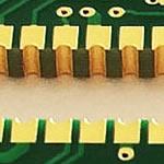
PCB Contract manufacturer, PCB Fabrication, Turnkey assembly services
Buy Print circuit board, customer: /USA/UK/Canada/South Africa...
powerPCB PCB design layout tools
-
powerPCB PCB design layout tools
Take your design from concept to creation with PADS
VX.2 now available! See what's new
Schematic Design
Integrated schematic capture for creative, top-quality, electronic product design.
PADS Standard/Standard Plus
PADS Professional
Analog/Mixed-Signal Circuit Simulation
Design, simulate, and analyze mixed-technology circuits with PADS AMS desktop and cloud-based solutions.
AMS Simulation Overview
PADS AMS Design Suite
Simulation & Analysis
Analyze, solve, and verify critical design requirements during product creation.
PADS Standard/Standard Plus
PADS Professional
Constraint Management
Manage hierarchical rules that drive correct-by-construction design.
PADS Standard/Standard Plus
PADS Professional
Data Management
Build and manage components and automate archive management.
PADS Professional
PCB Layout
Powerful PCB layout capabilities for easy design of printed circuit boards.
TUTORIAL 5389
Layout Considerations for High-Power Circuits
By: Shasta Thomas, Applications Engineer
Bill Quach, Applications Engineer
Abstract: As consumer devices continue to shrink in size, power considerations and appropriate thermal design become increasingly important for circuit designers and board layout engineers. This tutorial helps designers to ensure that a board is both electrically sound and thermally balanced for proper operation and optimum efficiency.
A similar version of this article appeared in the October 31, 2011 issue of EDN.
A Quick Thermal Tutorial
In general, thermal equations for semiconductor devices can be modeled after electrical equations, such that the well known and beloved Ohm's Law (V = I × R) becomes ΔT = P × θ, where ΔT is the thermal differential in °C, P is the power in watts, and θ is the thermal impedance (°C/W). For semiconductor devices, ΔT is the temperature differential from the junction of the device (e.g., the hottest point in the die) and another point (e.g., the case, ambient air, or board), and the thermal impedance, θ, is the thermal resistance from one point to another. Thermal impedance is often measured from the junction of an IC to another point (the ambient air, package, case, or board) and is described as junction-to-ambient resistance, θJA, junction-to-case resistance, θJC, or junction-to-board resistance, θJB, in data sheets (Figure 1).
Figure 1. Semiconductor IC thermal impedances can be modeled in much the same way as electrical circuits, as described by Ohm's Law.
Figure 1. Semiconductor IC thermal impedances can be modeled in much the same way as electrical circuits, as described by Ohm's Law.
Good thermal design is required to keep a device operating within safe temperature limits. The junction temperature, TJ, for an IC can be calculated as TJ = TA + (P × θJA) and it should never exceed the limit listed in the manufacturer's data sheet (generally ranging from +125°C to +175°C). Thermal impedance values also should be obtained from the original manufacturer, as they are both highly package and device dependent.
It is important to note that, while thermal equations can be modeled as electrical equations, the expected accuracy when working with electricity does not hold true for thermal operation. Often, actual thermal characteristics can vary as much as 30% from the calculated value.
Power Considerations for the Board
Board layout should be considered from the very beginning of a design. The most important rule for high power circuit boards is to know your power path. The location and amount of power flowing through a circuit is a major factor when deciding the IC position and type and amount of heat dissipation required on the printed circuit board (PCB).
Visit PADS.com for in-depth information on PADS features, learn how customers are using PADS to power PCB design, and to try PADS for yourself.
Visit PADS.com
QUICKLINKS TO PADS.COM RESOURCES
Try PADS Professional
Test-drive PADS' most powerful software option, designed for the independent, multi-discipline hardware engineer who does it all.
Try PADS Standard Plus
Learn how PADS Standard Plus delivers intuitive, easy-to-use schematic design and layout in our highest value, production-proven tools.
Where to buy PADS
Find the nearest PADS sales office, or locate a PADS reseller.
PADS downloads
Download viewers and request evaluation software.
Take PADS training
Take PADS courses in the classroom or online.
Find PADS support
Fast help from experienced PADS experts on SupportNet.
PCB Design, Analysis, & Package Integration
Xpedition Enterprise
Xpedition IC Packaging Design
HyperLynx
PCB Resource Center
All PCB Design Products
PCB SOFTWARE
DFM Validation & NPI
Valor NPI ensures a smooth transition from PCB design to fabrication, and on to assembly. The Valor NPI platform provides comprehensive DFM analysis, applied in parallel with your design flow for maximum... View Product Overview
Many factors affect the amount of layout for a given design. These factors include:
The amount of power flowing through the circuit
The ambient temperature around the device and the board
The amount of airflow around the device and the board
The board material
IC density on the board
Component Placement
Analog circuits and mixed-signal circuit boards generally include high-power analog blocks and sensitive digital or low-power analog blocks. Begin the layout by designing and placing power blocks. Keep connections in individual power blocks short and wide and ensure against unnecessary ground loops and noise generation. Multiple tutorials and application notes have been written about layout techniques and recommendations for high power circuits.1,2,3 In general, remember to:
Identify and reduce current loops, especially high current paths.
Limit resistive voltage drops and other parasitics between components.
Locate high-power circuitry away from sensitive circuitry.
Use good grounding techniques.
Power Supply PCB Designer / Layout Expert
Print Friendly
True Power Research is a power electronics consultant and provider of custom power supply designs. Part of our service and expertise is the design of PCB’s for electronic power supplies.
PCB design is a critical stage in the development of power supplies. The large switching currents are orders of magnitude greater than the sensitive control signal currents used to control the supply. Commingling these very large currents with the small control currents will almost always result in misbehavior. Additionally it is a key consideration to mitigation of both output and input noise. PCB layout of power electronics requires special understanding of how supplies operate along with understanding of all the usual parasitic elements usually operative at switching frequencies.
PCB Design Process for Power Supplies
The general work flow for power PCB layout is shown in the following flow chart:
Power PCB Design
Power Supply PCB Design Work Flow Process Chart
Definitions of PCB Layout Process
Netlist — Information detailing how the electronic parts are interconnected to accheive their functional purpose. The netlist becomes one of the inputs to the PCB document.
Schematic Capture — the process of representing the electronic design in schematic diagram form, from which a netlist of connectivity can be created.
Component Footprint — a 2D representation of the space a component will occupy on the PCB.
PCB Outline — The geographical boundary a PCB assumes and is the limit within which electronic components must be placed.
Layer Structure — Also known as the layer stackup, the arrangement of fiberglass and copper conducting layers which make up the board. There may be numerous internal conducting layers.
Part Placement — The process of locating parts on the PCB. This step in an important step and if done well and thoughtfully will greatly facilitate the successful completion of the board. Therefore, this step should take a significant portion of the PCB layout effort.
Planes — Layers of solid copper dedicated to a common net such as signal common. PCB layout software usually represent planes using inverse video.
Tips on how to properly design/layout a Printed Circuit Board (PCB)
Sections
General tips
Make important nodes accessible
Give space between components
Place components with the same orientation
Print the layout to see if components' sizes match
Exchange wiring directions between layers
Select the width of lines depending on current
Know the specifications of the manufacturer
Avoid 90º angles with traces
Use the silk layer
Use the schematic vs. layout comparison
Create a ground plane
Place bypass capacitors
Route the differential signal traces in parallel
Consider spots of heat
Make parallel footprints for hard to find components
Tips for power circuits
Keep power and control grounds separate
Use an inner layer for the control ground
Make power traces wider to withstand higher currents
Tips for mixed-signal circuits
Keep digital and analog grounds separate
Protect analog grounds from noise
Tips for PCB mounting
Solder from small to large components
Be aware of cold solder joints
Use flux for easy soldering
Do not trust the multimeter continuity test
General tips
Make important nodes accessible
It will eventually happen that you are trying to figure out why something is not working and you want to measure a signal inside your PCB. Before designing the PCB, you should think which points will be important to troubleshoot your circuit and, in case they are not easily accessible, add a test point somewhere connected to them. There are various forms of test points, but the ones that form a loop are great for test probes with hooks.
Test point #1 Test point #2 Test point #3
Give space between components
It is tempting to pack the components as close as possible, only to realize that there is no room for the routing of wires. Give some space between components so that wires can spread. The more pins the component has, the more space it will need. Spacing will not only facilitate auto-routing as it will make soldering easier.
Spacing between components
Place components with the same orientation
Components generally have a standard pin numbering, with pin #1 in the upper-left corner. If all components are oriented equally, you will not make mistakes when soldering or when inspecting a component.
Print the layout to see if components' sizes match
After laying out all the components, print out the layout. Place each component on top of the layout paper to see if they match. Sometimes datasheets may have errors.
Exchange wiring directions between layers
Draw vertical traces on one side and horizontal traces on the other. This facilitates wiring of lines that have to cross over the others. For multiple layers, alternate between directions.
Select the width of lines depending on current
Larger width reduces resistance, which in turn reduces the heat caused by dissipation. The width of the lines should be sized according to the estimated current that flows through them. You can use this online calculator to calculate their width. Therefore, power lines should be wider because all the current is supplied by these wires.
Know the specifications of the manufacturer
Each manufacturer has its own specifications, such as minimum trace width, spacing, number of layers, etc. Before starting design, you should consider what you need and find a manufacturer that meets your requirements. Your requirements also include the grade of materials of the PCB. There are grades ranging from FR-1 (paper-phenolic mixture) up to FR-5 (glass cloth and epoxy). Most PCB prototyping manufacturers use the FR-4, but FR–2 is used in high-volume consumer applications. The type of material affects the circuit board's strength, durability, moisture absorption and Flame Resistance (FR).
PCB Layout Design
We use Altium Designer for PCB layout design. Schematic file with full PCB footprint libraries are needed for layout design. DRC checks are performed as part of design service. Fabrication ready Gerber files and .PCBDOC file are sent to customers. Minor changes will be performed according to customer need for free after design delivery
PCB Schematic Design
Our designers will communicate with you to learn exactly what functionalities you would like to achieve for your product. Whether it is simple digital circuit, mixed signal circuit or RF circuit, we have the expertise needed for your design.
schematic
firmware
MCU Firmware Design
We provide firmware design for most mainstream MCUs. The popular MCUs we use in our designs include Texas Instrument MSP430, Microchip PIC and Atmel SAM ARM series. Our firmware design include all control functionalities, USB/UART/SPI links, etc. All source code will be delivered to customers.
Avoid 90º angles with traces
Routing — The process of placing interconnecting traces between parts.
Copper Pours — Smaller regions or polygons of solid copper used for various purposes such as shielding, heat transfer, etc. In power electronics, copper pours are often inhabited by thermal vias for heat transfer to other layers.
Furthermore, avoid collecting multiple power components together on a PCB. Placing these heat-generating components evenly over the board maximizes the thermal balance of the board and protects the PCB from warping. Efficiently reducing heat on the board also protects other sensitive circuitry and signals during operation.
PCB Supplier Shenzhen, China, PCB Manufacturer, Turnkey services
-
PCBSINO is the Top 5 PCB manufacturer company in China.
PCBSINO do rapid Prototype within 24 hours. we can make Flexible Print circuit boards and Rigid circuit boards, like FR4, High TG FR4, Rogers 4003, 4350,Al Aluminum metal Core MCPCB, Al2O3 Ceramic,Taconic,Halogen Free material, CEM-3, Fr2, CEM-1, CEM-2, 94VO, Rogers HF material, Polymide,Flexible PCB FPC etc.
we already made many type electronic product for our customer, Our turkey services team can source original components part for your project, senior Electronic engineer will follow each step of the production and do function test in PCB house.
Express PCB |
|
Rigid PCB Rapid Prototype,24 hours |
| Fr4 PCB |
|
prototype Lower to 15USD ! |
| Rapid Prototype |
|
Fr4 Rigid PCB Rapid Prototype China, |
Turnkey Services |
|
Turnkey PCB Assembly Services, |
| Turnkey services |
|
Print circuit board Manufacturing, Turnkey Services |
| Turnkey Assembly |
|
Through Hole PCB components wave soldering Assembly |
For furhter information, please feel free to contact us, www.pcbsino.com